bq24735
www.ti.com
SLUSAK9 –SEPTEMBER 2011
APPLICATION INFORMATION
Negative Output Voltage Protection
Reversely insert the battery pack into the charger output during production or hard shorts on battery to ground
will generate negative output voltage on SRP and SRN pin. IC internal electrostatic-discharge (ESD) diodes from
GND pin to SRP or SRN pins and two anti-parallel (AP) diodes between SRP and SRN pins can be forward
biased and negative current can pass through the ESD diodes and AP diodes when output has negative voltage.
Insert two small resistors for SRP and SRN pins to limit the negative current level when output has negative
voltage. Suggest resistor value is 10 ohm for SRP pin and 7-8 Ω for SRN pin. After adding small resistors, the
suggested pre-charge current is at least 192mA for a 10m ohm current sensing resistor. Another method is using
a small diode parallel with output capacitor, when battery connection is reversed the diode turns on and limits the
negative voltage level. Using diode protection method without insertion of small resistors into SRP and SRN pin
can get the best charging current accuracy.
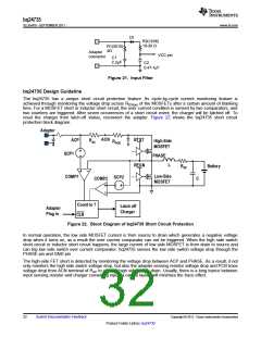
Reverse Input Voltage Protection
Q6, R12 and R13 in Figure 1 gives system and IC protection from reversed adapter voltage. In normal operation,
Q6 is turned off by negative Vgs. When adapter voltage is reversed, Q6 Vgs is positive. As a result, Q6 turns on
to short gate and source of Q2 so that Q2 is off. Q2 body diode blocks negative voltage to system. However,
CMSRC and ACDRV pins need R10 and R11 to limit the current due to the ESD diode of these pins when turned
on. Q6 must has low Vgs threshold voltage and low Qgs gate charge so it turns on before Q2 turns on. R10 and
R11 must have enough power rating for the power dissipation when the ESD diode is on. In Figure 2, the
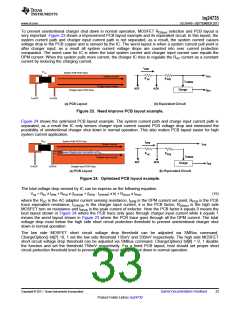
Schottky diode D3 gives the reverse adapter voltage protection, no extra small MOSFET and resistors are
needed.
In Figure 3, the Schottky diode Din is used for the reverse adapter voltage protection.
Reduce Battery Quiescent Current
When the adapter is not present, if VCC is powered with voltage higher than UVLO directly or indirectly (such as
through a LDO or switching converter) from battery, the internal BATFET charge pump gives the BATFET pin 6V
higher voltage than the SRN pin to drive the n-channel BATFET. As a result, the battery has higher quiescent
current. This is only necessary when the battery powers the system due to a high system current that goes
through the MOSFET channel instead of the body diode to reduce conduction loss and extend the battery
working life. When the system is totally shutdown, it is not necessary to let the internal BATFET charge pump
work. The host controller can use a digital signal EN to disconnect the battery power path to the VCC pin by U2
in Figure 1. As a result, battery quiescent current can be minimized. The host controller still can get power from
BATFET body diode because the total system current is the lowest when the system is shutdown, so there is no
high conduction loss of the body diode.
Inductor Selection
The bq24735 has three selectable fixed switching frequency. Higher switching frequency allows the use of
smaller inductor and capacitor values. Inductor saturation current should be higher than the charging current
(ICHG) plus half the ripple current (IRIPPLE):
ISAT ³ ICHG + (1/2) IRIPPLE
(4)
The inductor ripple current depends on input voltage (VIN), duty cycle (D = VOUT/VIN), switching frequency (fS) and
inductance (L):
V
´ D ´ (1 - D)
IN
IRIPPLE
=
fS ´ L
(5)
The maximum inductor ripple current happens with D = 0.5 or close to 0.5. For example, the battery charging
voltage range is from 9V to 12.6V for 3-cell battery pack. For 20V adapter voltage, 10V battery voltage gives the
maximum inductor ripple current. Another example is 4-cell battery, the battery voltage range is from 12V to
16.8V, and 12V battery voltage gives the maximum inductor ripple current.
Usually inductor ripple is designed in the range of (20-40%) maximum charging current as a trade-off between
inductor size and efficiency for a practical design.
Copyright © 2011, Texas Instruments Incorporated
Submit Documentation Feedback
29
Product Folder Link(s) :bq24735

 TI [ TEXAS INSTRUMENTS ]