bq24735
www.ti.com
SLUSAK9 –SEPTEMBER 2011
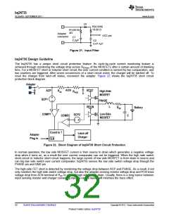
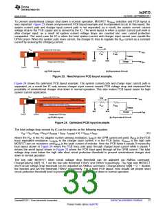
To prevent unintentional charger shut down in normal operation, MOSFET RDS(on) selection and PCB layout is
very important. Figure 23 shows a improvement PCB layout example and its equivalent circuit. In this layout, the
system current path and charger input current path is not separated, as a result, the system current causes
voltage drop in the PCB copper and is sensed by the IC. The worst layout is when a system current pull point is
after charger input; as a result all system current voltage drops are counted into over current protection
comparator. The worst case for IC is when the total system current and charger input current sum equals the
DPM current. When the system pulls more current, the charger IC tries to regulate the RAC current as a constant
current by reducing the charging current.
I
DPM
R AC
System Path PCB Trace
I
System current
SYS
R
R
AC
PCB
I
CHRGIN
Charger input current
ACP
ACN
Charger
I
Charger Input PCB Trace
BAT
To ACP
To ACN
(a) PCB Layout
(b) Equivalent Circuit
Figure 23. Need improve PCB layout example.
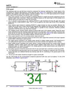
Figure 24 shows the optimized PCB layout example. The system current path and charge input current path is
separated, as a result the IC only senses charger input current caused PCB voltage drop and minimized the
possibility of unintentional charger shut down in normal operation. This also makes PCB layout easier for high
system current application.
R AC
System Path PCB Trace
I
DPM
I
System current
SYS
Single point connection at RAC
Charger input current
R
R
PCB
AC
I
CHRGIN
ACP
ACN
I
Charger
(b) Equivalent Circuit
BAT
To ACP
To ACN
Charger Input PCB Trace
(a) PCB Layout
Figure 24. Optimized PCB layout example.
The total voltage drop sensed by IC can be express as the following equation.
Vtop = RAC x IDPM + RPCB x (ICHRGIN + (IDPM - ICHRGIN) x k) + RDS(on) x IPEAK
(15)
where the RAC is the AC adapter current sensing resistance, IDPM is the DPM current set point, RPCB is the PCB
trace equivalent resistance, ICHRGIN is the charger input current, k is the PCB factor, RDS(on) is the high side
MOSFET turn on resistance and IPEAK is the peak current of inductor. Here the PCB factor k equals 0 means the
best layout shown in Figure 24 where the PCB trace only goes through charger input current while k equals 1
means the worst layout shown in Figure 23 where the PCB trace goes through all the DPM current. The total
voltage drop must below the high side short circuit protection threshold to prevent unintentional charger shut
down in normal operation.
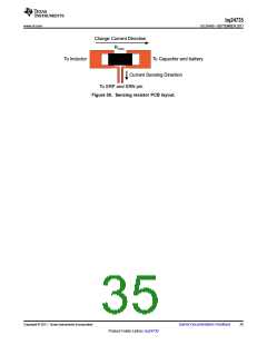
The low side MOSFET short circuit voltage drop threshold can be adjusted via SMBus command.
ChargeOption() bit[7] =0, 1 set the low side threshold 135mV and 230mV respectively. The high side MOSFET
short circuit voltage drop threshold can be adjusted via SMBus command. ChargeOption() bit[8] = 0, 1 disable
the function and set the threshold 750mV respectively. For a fixed PCB layout, host should set proper short
circuit protection threshold level to prevent unintentional charger shut down in normal operation.
Copyright © 2011, Texas Instruments Incorporated
Submit Documentation Feedback
33
Product Folder Link(s) :bq24735

 TI [ TEXAS INSTRUMENTS ]