bq24735
SLUSAK9 –SEPTEMBER 2011
www.ti.com
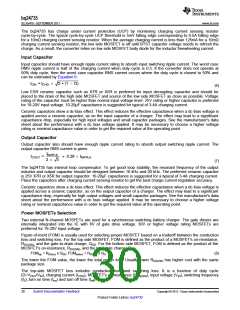
D1
R2(1206)
10-20 Ω
R1(2010)
2Ω
Adapter
connector
VCC pin
C1
2.2μF
C2
0.47-1μF
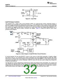
Figure 21. Input Filter
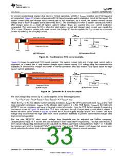
bq24735 Design Guideline
The bq24735 has a unique short circuit protection feature. Its cycle-by-cycle current monitoring feature is
achieved through monitoring the voltage drop across RDS(on) of the MOSFETs after a certain amount of blanking
time. For a MOSFET short or inductor short circuit, the over current condition is sensed by two comparators, and
two counters are triggered. After seven occurrences of a short circuit event, the charger will be latched off. To
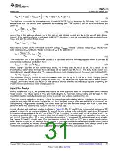
reset the charger from latch-off status, reconnect the adapter. Figure 22 shows the bq24735 short circuit
protection block diagram.
Adapter
ACN
BTST
ACP
SCP1
RAC
High-Side
MOSFET
RPCB
PHASE
L
REGN
RDC
Battery
Low-Side
MOSFET
COMP1
SCP2
COMP2
C
Count to 7
CLR
Latch off
Charger
Adapter
Plug in
Figure 22. Block Diagram of bq24735 Short Circuit Protection
In normal operation, the low side MOSFET current is from source to drain which generates a negative voltage
drop when it turns on, as a result the over current comparator can not be triggered. When the high side switch
short circuit or inductor short circuit happens, the large current of low side MOSFET is from drain to source and
can trig low side switch over current comparator. bq24735 senses the low side switch voltage drop through the
PHASE pin and GND pin.
The high-side FET short is detected by monitoring the voltage drop between ACP and PHASE. As a result, it not
only monitors the high side switch voltage drop, but also the adapter sensing resistor voltage drop and PCB trace
voltage drop from ACN terminal of RAC to charger high side switch drain. Usually, there is a long trance between
input sensing resistor and charger converting input, a careful layout will minimize the trace effect.
32
Submit Documentation Feedback
Copyright © 2011, Texas Instruments Incorporated
Product Folder Link(s) :bq24735

 TI [ TEXAS INSTRUMENTS ]