bq24160, bq24161
bq24163, bq24168
www.ti.com
SLUSAO0A –NOVEMBER 2011–REVISED MARCH 2012
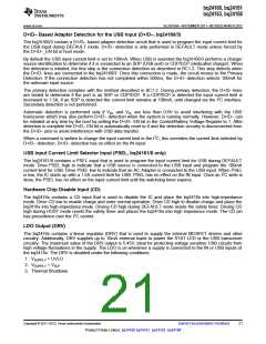
D+/D– Based Adapter Detection for the USB Input (D+/D–, bq24160/3)
The bq24160/3 contain a D+/D– based adapter detection circuit that is used to program the input current limit for
the USB input during DEFAULT mode. D+/D– detection is only performed in DEFAULT mode unless forced by
the D+/D–_EN bit in host mode.
By default the USB input current limit is set to 100mA. When USB is asserted the bq24160/3 performs a charger
source identification to determine if it is connected to an SDP (USB port) or CDP/DCP (dedicated charger). When
the detection is initated, the first step is the connection detection as described in BC1.2. This step detects when
the D+/D- lines are connected to the bq24160/3. Once this connection is made, the circuit moves to the Primary
Detection. If the connection detection has not completed within 500ms, the D+/D- detection selects 100mA for
the unknown input source.
The primary detection complies with the method described in BC1.2. During primary detection, the D+/D- lines
are tested to determine if the port is an SDP or CDP/DCP. If a CDP/DCP is detected the input current limit is
increased to 1.5A, if an SDP is detected the current limit remains at 100mA, until changed via the I2C interface.
Secondary detection is not performed.
Automatic detection is performed only if VD+ and VD– are less than 0.6V to avoid interfering with the USB
transceiver which may also perform D+/D– detection when the system is running normally. However, D+/D– can
be initiated at any time by the host by setting the D+/D– EN bit in the Control/Battery Voltage Register to 1. After
detection is complete the D+/D– EN bit is automatically reset to 0 and the detection circuitry is disconnected from
the D+/D– pins to avoid interference with USB data transfer.
When a command is written to change the input current limit in the I2C, this overrides the current limit selected by
D+/D– detection. D+/D– detection has no effect on the IN input.
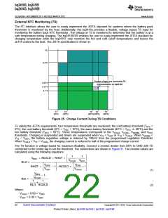
USB Input Current Limit Selector Input (PSEL, bq24161/8 only)
The bq24161/8 contains a PSEL input that is used to program the input current limit for USB during DEFAULT
mode. Drive PSEL high to indicate that a USB source is connected to the USB input and program the 100mA
current limit for USB. Drive PSEL low to indicate that an AC Adapter is connected to the USB input. When PSEL
is low, the IC starts up with a 1.5A current limit for USB. PSEL has no effect on the IN input. Once an I2C write is
done, the PSEL has no effect on the input current limit until the watchdog timer expires.
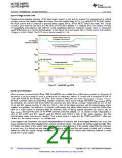
Hardware Chip Disable Input (CD)
The bq2416x contains a CD input that is used to disable the IC and place the bq2416x into high-impedance
mode. Drive CD low to enable charge and enter normal operation. Drive CD high to disable charge and place the
bq2416x into high-impedance mode. Driving CD high during DEFAULT mode resets the safety timer. Driving CD
high during HOST mode resets the safety timer and places the bq2416x into high impedance mode. The CD pin
has precedence over the I2C control.
LDO Output (DRV)
The bq2416x contains a linear regulator (DRV) that is used to supply the internal MOSFET drivers and other
circuitry. Additionally, DRV supplies up to 10mA external loads to power the STAT LED or the USB transceiver
circuitry. The maximum value of the DRV output is 5.45V; ideal for protecting voltage sensitive USB circuits from
high voltage fluctuations in the supply. The LDO is on whenever a supply is connected to the IN or USB inputs of
the bq2416x. The DRV is disabled under the following conditions:
1. VSUPPLY < UVLO
2. VSUPPLY < VSLP
3. Thermal Shutdown
Copyright © 2011–2012, Texas Instruments Incorporated
Submit Documentation Feedback
21
Product Folder Link(s): bq24160 bq24161 bq24163 bq24168

 TI [ TEXAS INSTRUMENTS ]