bq20z45
SLUS800–MARCH 2009 .................................................................................................................................................................................................. www.ti.com
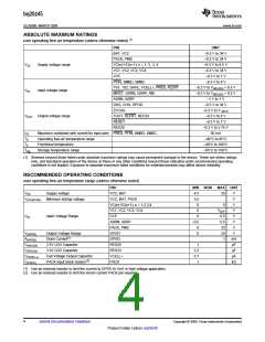
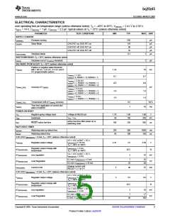
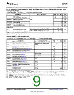
ABSOLUTE MAXIMUM RATINGS
over operating free-air temperature (unless otherwise noted)
(1)
PIN
UNIT
–0.3 V to 34 V
–0.3 V to 34 V
–0.3 V to 8.5 V
–0.3 V to 34 V
–0.3 V to 1 V
BAT, VCC
PACK, PMS
VSS
Supply voltage range
Input voltage range
VC(n)-VC(n+1); n = 1, 2, 3, 4
VC1, VC2, VC3, VC4
VC5
PFIN, SMBD, SMBC
TS1, TS2, SAFE, VCELL+, PRES; ALERT
MRST, GSRN, GSRP, RBI
ASRN, ASRP
–0.3 V to 6 V
–0.3 V to V(REG25) + 0.3 V
–0.3 V to V(REG25) + 0.3 V
–1 V to 1 V
VIN
DSG, CHG, GPOD
ZVCHG
–0.3 V to 34 V
–0.3 V to V (BAT)
–0.3 V to 6 V
VOUT Output voltage range
TOUT, ALERT, REG33
RESET
–0.3 V to 7 V
REG25
–0.3 V to 2.75 V
50 mA
ISS
TA
Maximum combined sink current for input pins PRES, PFIN, SMBD, SMBC
Operating free-air temperature range
Functional temperature
–40°C to 85°C
–40°C to 100°C
–65°C to 150°C
TF
Tstg
Storage temperature range
(1) Stresses beyond those listed under absolute maximum ratings may cause permanent damage to the device. These are stress ratings
only, and functional operation of the device at these or any other conditions beyond those indicated under recommended operating
conditions is not implied. Exposure to absolute-maximum-rated conditions for extended periods may affect device reliability.
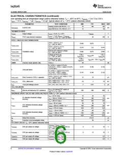
RECOMMENDED OPERATING CONDITIONS
over operating free-air temperature range (unless otherwise noted)
PIN
MIN NOM
MAX UNIT
VSS
Supply voltage
VCC, BAT
VCC, BAT, PACK
VC(n)-VC(n+1); n = 1,2,3,4
VC1, VC2, VC3, VC4
VC5
4.5
5.5
0
25
V
V
V(STARTUP)
Minimum startup voltage
5
VSUP
0.5
0.5
25
V
0
V
VIN
Input Voltage Range
0
V
ASRN, ASRP
PACK, PMS
GPOD
–0.5
0
V
V
V(GPOD)
A(GPOD)
C(REG25)
C(REG33)
C(VCELL+)
C(PACK)
Output Voltage Range
Drain Current(1)
0
25
V
GPOD
1
mA
µF
µF
µF
kΩ
2.5V LDO Capacitor
REG25
1
2.2
0.1
1
3.3V LDO Capacitor
REG33
Cell Voltage Output Capacitor
PACK input block resistor(2)
VCELL+
PACK
(1) Use an external resistor to limit the current to GPOD to 1mA in high voltage application.
(2) Use an external resistor to limit the inrush current PACK pin required.
4
Submit Documentation Feedback
Copyright © 2009, Texas Instruments Incorporated
Product Folder Link(s): bq20z45

 TI [ TEXAS INSTRUMENTS ]