AM6548, AM6528, AM6526
ZHCSLA7B –DECEMBER 2019 –REVISED JUNE 2021
www.ti.com.cn
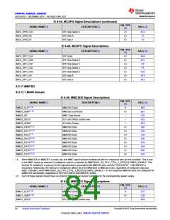
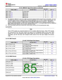
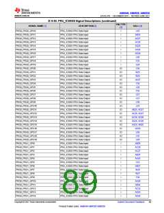
表6-47. MMCSD1 Signal Descriptions (continued)
PIN TYPE
SIGNAL NAME [1]
DESCRIPTION [2]
BALL [4]
[3]
MMC1_SDWP
SD Write Protect
MMC/SD Data
MMC/SD Data
MMC/SD Data
MMC/SD Data
I
C24
D28
E27
D26
D27
MMC1_DAT0(1) (2)
MMC1_DAT1(1) (2)
MMC1_DAT2(1) (2)
MMC1_DAT3(1) (2)
IO
IO
IO
IO
(1) When MMCSD0 or MMCSD1 is used, any non-MMC signal function multiplexed with the respective pins are not available. This is due
to the MMC having an internal IO multiplexer which is controlled by MMCSD0/1_SS_PHY_CTRL_1_REG[31] IOMUX_ENABLE. This
internal IO multiplexer is primary for the signal functions associated with MMCSD pins, and the PADCONFIG’s MUXMODE is
secondary. Additionally, the internal IO multiplexer affects all of the MMCSD0 or MMCSD1 pins, regardless of configured data bus
width. Therefore, when MMCSD0/1_SS_PHY_CTRL_1_REG[31] IOMUX_ENABLE = 0, the respective MMCSD pins are configured for
eMMC/SD functionality, regardless of the PADCONFIG [MUXMODE] setting.
(2) Each of these signals should have an external 50kΩpull-up resistor connected to the corresponding power supply.
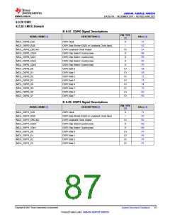
6.3.18 CPTS
Note
Some CPTS signals are connected directly to CPTS modules within the device. Other CPTS signals
are connected to the Time Sync Router and fanned out to peripherals linked to the router. Input
signals are sent to the peripherals while output signals are sourced from the peripherals. For more
information, see the Time Sync and Compare Events section in the Time Sync chapter in the device
TRM.
6.3.18.1 MCU Domain
表6-48. CPTS0 Signal Descriptions
PIN TYPE
SIGNAL NAME [1]
MCU_CPTS0_RFT_CLK
DESCRIPTION [2]
CPTS Reference Clock
BALL [4]
AB3
[3]
I
CPTS Time Stamp Counter Compare from
MCU_CPSW0_CPTS0
MCU_CPTS0_TS_COMP
MCU_CPTS0_TS_SYNC
MCU_CPTS0_HW1TSPUSH
MCU_CPTS0_HW2TSPUSH
O
O
I
AB4
CPTS Time Stamp Counter Bit from
MCU_CPSW0_CPTS0
AC5
AC2
AC1
CPTS Hardware Time Stamp Push 1 input to Time Sync
Router and MCU_CPSW0_CPTS0
CPTS Hardware Time Stamp Push 2 input to Time Sync
Router and MCU_CPSW0_CPTS0
I
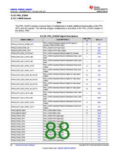
6.3.18.2 MAIN Domain
表6-49. CPTS0 Signal Descriptions
DESCRIPTION [2]
PIN TYPE
SIGNAL NAME [1]
CPTS0_RFT_CLK
BALL [4]
D21
[3]
CPTS Reference Clock
I
CPTS Time Stamp Counter Compare from
NAVSS0_CPTS0
CPTS0_TS_COMP
O
O
I
AF13
AG12
B21
CPTS0_TS_SYNC
CPTS Time Stamp Counter Bit from NAVSS0_CPTS0
CPTS Hardware Time Stamp Push 1 input to Time Sync
Router
CPTS0_HW1TSPUSH
CPTS Hardware Time Stamp Push 2 input to Time Sync
Router
CPTS0_HW2TSPUSH
SYNC0_OUT
I
E21
D21
CPTS Time Stamp Generator Bit 0 from Time Sync
Router
O
Copyright © 2021 Texas Instruments Incorporated
Submit Document Feedback
85
Product Folder Links: AM6548 AM6528 AM6526

 TI [ TEXAS INSTRUMENTS ]