AM6548, AM6528, AM6526
ZHCSLA7B –DECEMBER 2019 –REVISED JUNE 2021
www.ti.com.cn
6.3.23.3 WKUP Domain
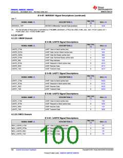
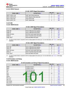
表6-62. UART0 Signal Descriptions
PIN TYPE
SIGNAL NAME [1]
DESCRIPTION [2]
UART Clear to Send (active low)
BALL [4]
[3]
WKUP_UART0_CTSn
WKUP_UART0_RTSn
WKUP_UART0_RXD
WKUP_UART0_TXD
I
AC2
AC1
AB1
AB5
UART Request to Send (active low)
UART Receive Data
O
I
UART Transmit Data
O
6.3.24 USB
6.3.24.1 MAIN Domain
表6-63. USB0 Signal Descriptions
PIN TYPE
SIGNAL NAME [1]
DESCRIPTION [2]
BALL [4]
[3]
USB0_DM
USB 2.0 Differential Data (negative)
USB 2.0 Differential Data (positive)
USB VBUS control output (active high)
USB 2.0 Dual-Role Device Role Select
USB Level-shifted VBUS Input
IO
IO
O
A
AE2
AF1
AD9
AF7
AE7
USB0_DP
USB0_DRVVBUS
USB0_ID
USB0_VBUS(1)
A
(1) An external resistor divider is required to limit the voltage applied to the device pin. For more information, see 节9.2.3, USB Design
Guidelines.
表6-64. USB1 Signal Descriptions
PIN TYPE
SIGNAL NAME [1]
DESCRIPTION [2]
BALL [4]
[3]
IO
IO
O
USB1_DM
USB1_DP
USB 2.0 Differential Data (negative)
USB 2.0 Differential Data (positive)
USB VBUS control output (active high)
USB 2.0 Dual-Role Device Role Select
USB Level-shifted VBUS Input
AD2
AE1
AC8
AF5
AF6
USB1_DRVVBUS
USB1_ID
USB1_VBUS(1)
A
A
(1) An external resistor divider is required to limit the voltage applied to the device pin. For more information, see 节9.2.3, USB Design
Guidelines.
6.3.25 Emulation and Debug
6.3.25.1 MAIN Domain
表6-65. Emulation and Debug 0 Signal Descriptions
PIN TYPE
SIGNAL NAME [1]
DESCRIPTION [2]
BALL [4]
[3]
IO
IO
I
EMU0
Emulation Control 0
Emulation Control 1
AA2
AA1
EMU1
TCK
JTAG Test Clock Input
JTAG Test Data Input
JTAG Test Data Output
JTAG Test Mode Select Input
JTAG Reset
AA4
TDI
I
C20
TDO
OZ
I
A20
TMS
A21
TRSTn
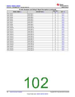
TRC_CLK
TRC_CTL
TRC_DATA0
TRC_DATA1
I
AA3
Trace Clock
O
O
O
O
AF18
AE18
AH17
AG18
Trace Control
Trace Data 0
Trace Data 1
Copyright © 2021 Texas Instruments Incorporated
Submit Document Feedback 101
Product Folder Links: AM6548 AM6528 AM6526

 TI [ TEXAS INSTRUMENTS ]