AM3359, AM3358, AM3357
AM3356, AM3354, AM3352
SPRS717F –OCTOBER 2011–REVISED APRIL 2013
www.ti.com
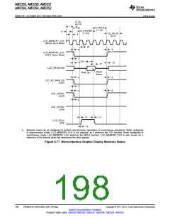
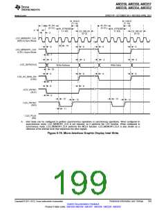
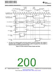
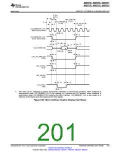
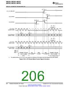
5.9.2 LCD Raster Mode
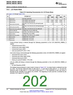
Table 5-76. Switching Characteristics for LCD Raster Mode
(see Figure 5-82 through Figure 5-85)
OPP50
MIN
OPP100
MIN
NO.
PARAMETER
UNIT
MAX
MAX
1
2
3
tc(LCD_PCLK)
tw(LCD_PCLKH)
tw(LCD_PCLKL)
Cycle time, pixel clock
15.8
0.45tc
0.45tc
7.9
ns
ns
ns
Pulse duration, pixel clock high
Pulse duration, pixel clock low
0.55tc
0.55tc
0.45tc
0.55tc
0.55tc
0.45tc
Delay time, LCD_PCLK to LCD_DATA[23:0] valid
(write)
4
5
td(LCD_PCLK-LCD_DATAV)
td(LCD_PCLK-LCD_DATAI)
3.0
1.9
ns
ns
Delay time, LCD_PCLK to LCD_DATA[23:0] invalid
(write)
-3.0
-1.7
6
7
8
9
td(LCD_PCLK-LCD_AC_BIAS_EN) Delay time, LCD_PCLK to LCD_AC_BIAS_EN
-3.0
0.5
-3.0
0.5
-3.0
0.5
0.5
0.5
3.0
2.4
3.0
2.4
3.0
2.4
2.4
2.4
-1.7
0.5
-1.7
0.5
-1.7
0.5
0.5
0.5
1.9
2.4
1.9
2.4
1.9
2.4
2.4
2.4
ns
ns
ns
ns
ns
ns
ns
ns
tt(LCD_AC_BIAS_EN)
td(LCD_PCLK-LCD_VSYNC)
tt(LCD_VSYNC)
Transition time, LCD_AC_BIAS_EN
Delay time, LCD_PCLK to LCD_VSYNC
Transition time, LCD_VSYNC
10 td(LCD_PCLK-LCD_HSYNC)
11 tt(LCD_HSYNC)
12 tt(LCD_PCLK)
Delay time, LCD_PCLK to LCD_HSYNC
Transition time, LCD_HSYNC
Transition time, LCD_PCLK
13 tt(LCD_DATA)
Transition time, LCD_DATA
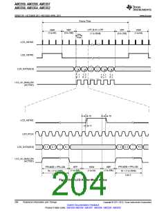
Frame-to-frame timing is derived through the following parameters in the LCD (RASTER_TIMING_1)
register:
•
•
•
•
Vertical front porch (VFP)
Vertical sync pulse width (VSW)
Vertical back porch (VBP)
Lines per panel (LPP_B10 + LPP)
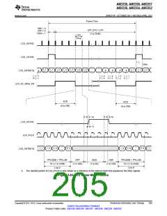
Line-to-line timing is derived through the following parameters in the LCD (RASTER_TIMING_0) register:
•
•
•
•
Horizontal front porch (HFP)
Horizontal sync pulse width (HSW)
Horizontal back porch (HBP)
Pixels per panel (PPLMSB + PPLLSB)
LCD_AC_BIAS_EN timing is derived through the following parameter in the LCD (RASTER_TIMING_2)
register:
•
AC bias frequency (ACB)
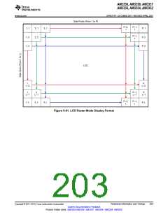
The display format produced in raster mode is shown in Figure 5-81. An entire frame is delivered one line
at a time. The first line delivered starts at data pixel (1, 1) and ends at data pixel (P, 1). The last line
delivered starts at data pixel (1, L) and ends at data pixel (P, L). The beginning of each new frame is
denoted by the activation of IO signal LCD_VSYNC. The beginning of each new line is denoted by the
activation of IO signal LCD_HSYNC.
202
Peripheral Information and Timings
Copyright © 2011–2013, Texas Instruments Incorporated
Submit Documentation Feedback
Product Folder Links: AM3359 AM3358 AM3357 AM3356 AM3354 AM3352

 TI [ TEXAS INSTRUMENTS ]