AM3359, AM3358, AM3357
AM3356, AM3354, AM3352
SPRS717F –OCTOBER 2011–REVISED APRIL 2013
5.6.2.2 DDR2 Routing Guidelines
5.6.2.2.1 Board Designs
www.ti.com
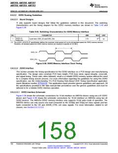
TI only supports board designs that follow the guidelines outlined in this document. The switching
characteristics and the timing diagram for the DDR2 memory interface are shown in Table 5-43 and
Figure 5-38.
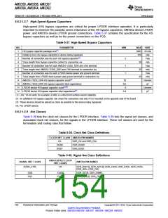
Table 5-43. Switching Characteristics for DDR2 Memory Interface
NO.
PARAMETER
MIN
MAX
UNIT
tc(DDR_CK)
tc(DDR_CKn)
1
Cycle time, DDR_CK and DDR_CKn
3.75
8(1)
ns
(1) The JEDEC JESD79-2F specification defines the maximum clock period of 8 ns for all standard-speed bin DDR2 memory devices.
Therefore, all standard-speed bin DDR2 memory devices are required to operate at 125 MHz.
1
DDR_CK
DDR_CKn
Figure 5-38. DDR2 Memory Interface Clock Timing
5.6.2.2.2 DDR2 Interface
This section provides the timing specification for the DDR2 interface as a PCB design and manufacturing
specification. The design rules constrain PCB trace length, PCB trace skew, signal integrity, cross-talk,
and signal timing. These rules, when followed, result in a reliable DDR2 memory system without the need
for a complex timing closure process. For more information regarding the guidelines for using this DDR2
specification, see the Understanding TI’s PCB Routing Rule-Based DDR Timing Specification application
report (literature number SPRAAV0). This application report provides generic guidelines and approach. All
the specifications provided in the data manual take precedence over the generic guidelines and must be
adhered to for a reliable DDR2 interface operation.
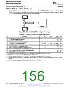
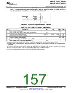
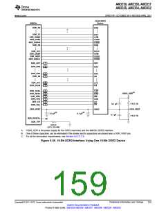
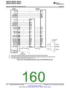
5.6.2.2.2.1 DDR2 Interface Schematic
Figure 5-39 shows the schematic connections for 16-bit interface on AM335x device using one x16 DDR2
device and Figure 5-40 shows the schematic connections for 16-bit interface on AM335x using two x8
DDR2 devices. The AM335x DDR2 memory interface only supports 16-bit wide mode of operation. The
AM335x device can only source one load connected to the DQS[x] and DQ[x] net class signals and two
loads connected to the CK and ADDR_CTRL net class signals. For more information related to net
classes, see Section 5.6.2.2.2.8.
158
Peripheral Information and Timings
Copyright © 2011–2013, Texas Instruments Incorporated
Submit Documentation Feedback
Product Folder Links: AM3359 AM3358 AM3357 AM3356 AM3354 AM3352

 TI [ TEXAS INSTRUMENTS ]