AM3359, AM3358, AM3357
AM3356, AM3354, AM3352
www.ti.com
SPRS717F –OCTOBER 2011–REVISED APRIL 2013
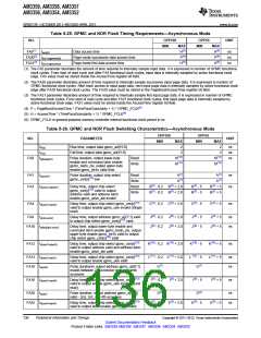
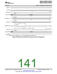
Table 5-26. GPMC and NOR Flash Switching Characteristics—Asynchronous Mode (continued)
OPP100
OPP50
MIN
F(6) - 5
NO.
PARAMETER
UNIT
MIN
MAX
MAX
F(6) + 5
FA27 td(csnV-wenIV)
Delay time, output chip select gpmc_csn[x](13)
valid to output write enable gpmc_wen invalid
F(6) - 0.2
F(6) + 2.0
ns
FA28 td(wenV-dV)
FA29 td(dV-csnV)
FA37 td(oenV-aIV)
Delay time, output write enable gpmc_ wen
valid to output data gpmc_ad[15:0] valid
2.0
5
J(9) + 5
5
ns
ns
ns
Delay time, output data gpmc_ad[15:0] valid to
output chip select gpmc_csn[x](13) valid
J(9) - 0.2
J(9) + 2.0
2.0
J(9) - 5
Delay time, output enable gpmc_oen valid to
output address gpmc_ad[15:0] phase end
(1) For single read: A = (CSRdOffTime - CSOnTime) * (TimeParaGranularity + 1) * GPMC_FCLK(14)
For single write: A = (CSWrOffTime - CSOnTime) * (TimeParaGranularity + 1) * GPMC_FCLK(14)
For burst read: A = (CSRdOffTime - CSOnTime + (n - 1) * PageBurstAccessTime) * (TimeParaGranularity + 1) * GPMC_FCLK(14)
For burst write: A = (CSWrOffTime - CSOnTime + (n - 1) * PageBurstAccessTime) * (TimeParaGranularity + 1) * GPMC_FCLK(14)
with n being the page burst access number
(2) For reading: B = ((ADVRdOffTime - CSOnTime) * (TimeParaGranularity + 1) + 0.5 * (ADVExtraDelay - CSExtraDelay)) *
GPMC_FCLK(14)
For writing: B = ((ADVWrOffTime - CSOnTime) * (TimeParaGranularity + 1) + 0.5 * (ADVExtraDelay - CSExtraDelay)) * GPMC_FCLK(14)
(3) C = ((OEOffTime - CSOnTime) * (TimeParaGranularity + 1) + 0.5 * (OEExtraDelay - CSExtraDelay)) * GPMC_FCLK(14)
(4) D = PageBurstAccessTime * (TimeParaGranularity + 1) * GPMC_FCLK(14)
(5) E = ((WEOnTime - CSOnTime) * (TimeParaGranularity + 1) + 0.5 * (WEExtraDelay - CSExtraDelay)) * GPMC_FCLK(14)
(6) F = ((WEOffTime - CSOnTime) * (TimeParaGranularity + 1) + 0.5 * (WEExtraDelay - CSExtraDelay)) * GPMC_FCLK(14)
(7) G = Cycle2CycleDelay * GPMC_FCLK(14)
(8) I = ((OEOffTime + (n - 1) * PageBurstAccessTime - CSOnTime) * (TimeParaGranularity + 1) + 0.5 * (OEExtraDelay - CSExtraDelay)) *
GPMC_FCLK(14)
(9) J = (CSOnTime * (TimeParaGranularity + 1) + 0.5 * CSExtraDelay) * GPMC_FCLK(14)
(10) K = ((ADVOnTime - CSOnTime) * (TimeParaGranularity + 1) + 0.5 * (ADVExtraDelay - CSExtraDelay)) * GPMC_FCLK(14)
(11) L = ((OEOnTime - CSOnTime) * (TimeParaGranularity + 1) + 0.5 * (OEExtraDelay - CSExtraDelay)) * GPMC_FCLK(14)
(12) For single read: N = RdCycleTime * (TimeParaGranularity + 1) * GPMC_FCLK(14)
For single write: N = WrCycleTime * (TimeParaGranularity + 1) * GPMC_FCLK(14)
For burst read: N = (RdCycleTime + (n - 1) * PageBurstAccessTime) * (TimeParaGranularity + 1) * GPMC_FCLK(14)
For burst write: N = (WrCycleTime + (n - 1) * PageBurstAccessTime) * (TimeParaGranularity + 1) * GPMC_FCLK(14)
(13) In gpmc_csn[x], x is equal to 0, 1, 2, 3, 4 or 5.
(14) GPMC_FCLK is general-purpose memory controller internal functional clock period in ns.
Copyright © 2011–2013, Texas Instruments Incorporated
Peripheral Information and Timings
137
Submit Documentation Feedback
Product Folder Links: AM3359 AM3358 AM3357 AM3356 AM3354 AM3352

 TI [ TEXAS INSTRUMENTS ]