AM3359, AM3358, AM3357
AM3356, AM3354, AM3352
SPRS717F –OCTOBER 2011–REVISED APRIL 2013
www.ti.com
UNIT
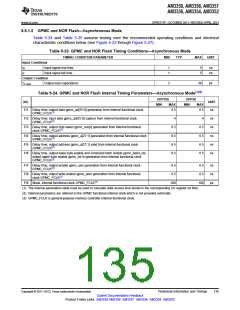
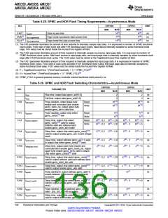
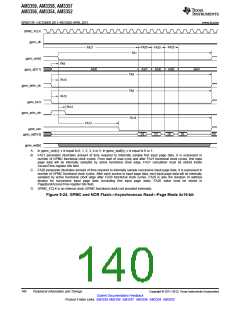
Table 5-25. GPMC and NOR Flash Timing Requirements—Asynchronous Mode
NO.
OPP100
MIN
OPP50
MIN
MAX
H(5)
P(4)
MAX
H(5)
P(4)
FA5(1) tacc(d)
Data access time
ns
ns
ns
FA20(2) tacc1-pgmode(d)
FA21(3) tacc2-pgmode(d)
Page mode successive data access time
Page mode first data access time
H(5)
H(5)
(1) The FA5 parameter illustrates the amount of time required to internally sample input data. It is expressed in number of GPMC functional
clock cycles. From start of read cycle and after FA5 functional clock cycles, input data is internally sampled by active functional clock
edge. FA5 value must be stored inside the AccessTime register bit field.
(2) The FA20 parameter illustrates amount of time required to internally sample successive input page data. It is expressed in number of
GPMC functional clock cycles. After each access to input page data, next input page data is internally sampled by active functional clock
edge after FA20 functional clock cycles. The FA20 value must be stored in the PageBurstAccessTime register bit field.
(3) The FA21 parameter illustrates amount of time required to internally sample first input page data. It is expressed in number of GPMC
functional clock cycles. From start of read cycle and after FA21 functional clock cycles, first input page data is internally sampled by
active functional clock edge. FA21 value must be stored inside the AccessTime register bit field.
(4) P = PageBurstAccessTime * (TimeParaGranularity + 1) * GPMC_FCLK(6)
(5) H = AccessTime * (TimeParaGranularity + 1) * GPMC_FCLK(6)
(6) GPMC_FCLK is general-purpose memory controller internal functional clock period in ns.
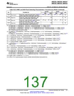
Table 5-26. GPMC and NOR Flash Switching Characteristics—Asynchronous Mode
OPP100
MIN
OPP50
MIN
NO.
PARAMETER
UNIT
MAX
2
MAX
2
tR(d)
Rise time, output data gpmc_ad[15:0]
Fall time, output data gpmc_ad[15:0]
ns
ns
ns
tF(d)
2
2
FA0
tw(be[x]nV)
Pulse duration, output lower-byte
enable and command latch enable
gpmc_be0n_cle, output upper-byte
enable gpmc_be1n valid time
Read
Write
N(12)
N(12)
N(12)
N(12)
FA1
FA3
tw(csnV)
Pulse duration, output chip select
gpmc_csn[x](13) low
Read
Write
Read
Write
A(1)
A(1)
B(2) + 2.0
B(2) + 2.0
A(1)
A(1)
B(2) + 5
B(2) + 5
ns
ns
td(csnV-advnIV)
Delay time, output chip select
gpmc_csn[x](13) valid to output
address valid and address latch
enable gpmc_advn_ale invalid
B(2) - 0.2
B(2) - 0.2
B(2) - 5
B(2) - 5
FA4
FA9
td(csnV-oenIV)
Delay time, output chip select gpmc_csn[x](13)
valid to output enable gpmc_oen invalid (Single
read)
C(3) - 0.2
C(3) + 2.0
C(3) - 5
C(3) + 5
ns
td(aV-csnV)
Delay time, output address gpmc_a[27:1] valid
to output chip select gpmc_csn[x](13) valid
J(9) - 0.2
J(9) - 0.2
J(9) + 2.0
J(9) + 2.0
J(9) - 5
J(9) - 5
J(9) + 5
J(9) + 5
ns
ns
FA10 td(be[x]nV-csnV)
Delay time, output lower-byte enable and
command latch enable gpmc_be0n_cle, output
upper-byte enable gpmc_be1n valid to output
chip select gpmc_csn[x](13) valid
FA12 td(csnV-advnV)
Delay time, output chip select gpmc_csn[x](13)
valid to output address valid and address latch
enable gpmc_advn_ale valid
K(10) - 0.2 K(10) + 2.0
K(10) - 5
K(10) + 5
ns
FA13 td(csnV-oenV)
FA16 tw(aIV)
Delay time, output chip select gpmc_csn[x](13)
valid to output enable gpmc_oen valid
L(11) - 0.2 L(11) + 2.0
G(7)
L
(11) - 5
G(7)
L(11) + 5
ns
ns
Pulse durationm output address gpmc_a[26:1]
invalid between 2 successive read and write
accesses
FA18 td(csnV-oenIV)
Delay time, output chip select gpmc_csn[x](13)
valid to output enable gpmc_oen invalid (Burst
read)
I(8) - 0.2
I(8) + 2.0
I(8) - 5
I(8) + 5
ns
FA20 tw(aV)
Pulse duration, output address gpmc_a[27:1]
valid - 2nd, 3rd, and 4th accesses
Delay time, output chip select gpmc_csn[x](13)
valid to output write enable gpmc_wen valid
D(4)
D(4)
ns
ns
FA25 td(csnV-wenV)
E(5) - 0.2
E(5) + 2.0
E(5) - 5
E(5) + 5
136
Peripheral Information and Timings
Copyright © 2011–2013, Texas Instruments Incorporated
Submit Documentation Feedback
Product Folder Links: AM3359 AM3358 AM3357 AM3356 AM3354 AM3352

 TI [ TEXAS INSTRUMENTS ]