AM3359, AM3358, AM3357
AM3356, AM3354, AM3352
www.ti.com
SPRS717F –OCTOBER 2011–REVISED APRIL 2013
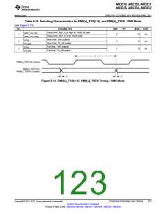
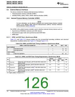
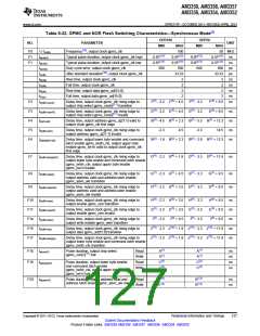
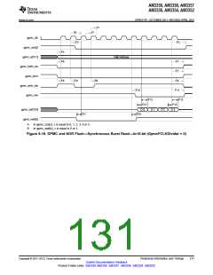
Table 5-22. GPMC and NOR Flash Switching Characteristics—Synchronous Mode(2)
OPP100
MIN
OPP50
MIN
NO.
PARAMETER
UNIT
MAX
MAX
F0
F1
F1
1 / tc(clk)
Frequency(15), output clock gpmc_clk
Typical pulse duration, output clock gpmc_clk high
Typical pulse duration, output clock gpmc_clk low
Duty cycle error, output clock gpmc_clk
Jitter standard deviation(16), output clock gpmc_clk
Rise time, output clock gpmc_clk
100
0.5P(12)
0.5P(12)
50 MHz
tw(clkH)
tw(clkL)
tdc(clk)
tJ(clk)
0.5P(12)
0.5P(12)
0.5P(12)
0.5P(12)
-500
0.5P(12)
0.5P(12)
ns
ns
ps
ps
ns
ns
ns
ns
ns
-500
500
500
33.33
33.33
tR(clk)
2
2
2
2
2
tF(clk)
Fall time, output clock gpmc_clk
2
tR(do)
Rise time, output data gpmc_ad[15:0]
Fall time, output data gpmc_ad[15:0]
2
2
tF(do)
F2
F3
F4
F5
F6
td(clkH-csnV)
Delay time, output clock gpmc_clk rising edge to
output chip select gpmc_csn[x](11) transition
F(6) - 2.2 F(6) + 4.5
E(5) - 2.2 E(5) + 4.5
B(2) - 4.5 B(2) + 2.3
F(6) - 3.2
E(5) - 3.2
F(6) + 9.5
td(clkH-csnIV)
td(aV-clk)
td(clkH-aIV)
td(be[x]nV-clk)
Delay time, output clock gpmc_clk rising edge to
output chip select gpmc_csn[x](11) invalid
E(5) + 9.5
ns
ns
ns
ns
Delay time, output address gpmc_a[27:1] valid to
output clock gpmc_clk first edge
B(2) - 5.5 B(2) + 12.3
-3.3 14.5
B(2) - 2.9 B(2) + 12.3
Delay time, output clock gpmc_clk rising edge to
output address gpmc_a[27:1] invalid
-2.3
4.5
Delay time, output lower byte enable and command
latch enable gpmc_be0n_cle, output upper byte
enable gpmc_be1n valid to output clock gpmc_clk
first edge
B(2) - 1.9 B(2) + 2.3
F7
td(clkH-be[x]nIV)
Delay time, output clock gpmc_clk rising edge to
output lower byte enable and command latch enable
gpmc_be0n_cle, output upper byte enable
gpmc_be1n invalid
D(4) - 2.3 D(4) + 1.9
D(4) - 3.3 D(4) + 11.9
ns
F8
F9
td(clkH-advn)
Delay time, output clock gpmc_clk rising edge to
output address valid and address latch enable
gpmc_advn_ale transition
G(7) - 2.3 G(7) + 4.5
D(4) - 2.3 D(4) + 3.5
G(7) - 3.3
D(4) - 3.3
G(7) + 9.5
D(4) + 9.5
ns
ns
td(clkH-advnIV)
Delay time, output clock gpmc_clk rising edge to
output address valid and address latch enable
gpmc_advn_ale invalid
F10
F11
F14
F15
F17
td(clkH-oen)
td(clkH-oenIV)
td(clkH-wen)
td(clkH-do)
Delay time, output clock gpmc_clk rising edge to
output enable gpmc_oen transition
H(8) - 2.3 H(8) + 3.5
E(5) - 2.3 E(5) + 3.5
H(8) - 3.3
E(5) - 3.3
I(9) - 3.3
H(8) + 8.5
E(5) + 8.5
I(9) + 9.5
ns
ns
ns
ns
ns
Delay time, output clock gpmc_clk rising edge to
output enable gpmc_oen invalid
Delay time, output clock gpmc_clk rising edge to
output write enable gpmc_wen transition
I(9) - 2.3
I(9) + 4.5
Delay time, output clock gpmc_clk rising edge to
output data gpmc_ad[15:0] transition
J(10) - 2.3 J(10) + 1.9 J(10) - 3.3 J(10) + 11.9
J(10) - 2.3 J(10) + 1.9 J(10) - 3.3 J(10) + 11.9
td(clkH-be[x]n)
Delay time, output clock gpmc_clk rising edge to
output lower byte enable and command latch enable
gpmc_be0n_cle transition
F18
F19
tw(csnV)
Pulse duration, output chip select
gpmc_csn[x](11) low
Read
Write
Read
Write
A(1)
A(1)
C(3)
C(3)
A(1)
A(1)
C(3)
C(3)
ns
ns
ns
ns
tw(be[x]nV)
Pulse duration, output lower byte enable
and command latch enable
gpmc_be0n_cle, output upper byte enable
gpmc_be1n low
F20
tw(advnV)
Pulse duration, output address valid and
address latch enable gpmc_advn_ale low
Read
Write
K(13)
K(13)
K(13)
K(13)
ns
ns
Copyright © 2011–2013, Texas Instruments Incorporated
Peripheral Information and Timings
127
Submit Documentation Feedback
Product Folder Links: AM3359 AM3358 AM3357 AM3356 AM3354 AM3352

 TI [ TEXAS INSTRUMENTS ]