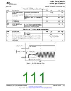
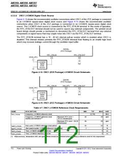
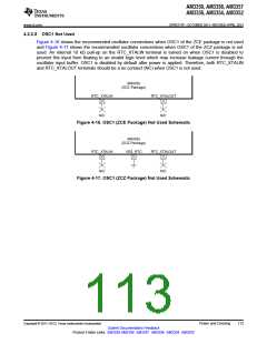
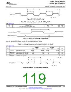
AM3359, AM3358, AM3357
AM3356, AM3354, AM3352
www.ti.com
SPRS717F –OCTOBER 2011–REVISED APRIL 2013
5 Peripheral Information and Timings
The AM335x device contains many peripheral interfaces. In order to reduce package size and lower
overall system cost while maintaining maximum functionality, many of the AM335x terminals can multiplex
up to eight signal functions. Although there are many combinations of pin multiplexing that are possible,
only a certain number of sets, called IO Sets, are valid due to timing limitations. These valid IO Sets were
carefully chosen to provide many possible application scenarios for the user.
Texas Instruments has developed a Windows-based application called Pin Mux Utility that helps a system
designer select the appropriate pin-multiplexing configuration for their AM335x-based product design. The
Pin Mux Utility provides a way to select valid IO Sets of specific peripheral interfaces to ensure the pin-
multiplexing configuration selected for a design only uses valid IO Sets supported by the AM335x device.
5.1 Parameter Information
The data provided in the following Timing Requirements and Switching Characteristics tables assumes the
device is operating within the Recommended Operating Conditions defined in Section 3, unless otherwise
noted.
5.1.1 Timing Parameters and Board Routing Analysis
The timing parameter values specified in this data manual do not include delays by board routings. As a
good board design practice, such delays must always be taken into account. Timing values may be
adjusted by increasing or decreasing such delays. TI recommends utilizing the available IO buffer
information specification (IBIS) models to analyze the timing characteristics correctly. If needed, external
logic hardware such as buffers may be used to compensate any timing differences.
The timing parameter values specified in this data manual assume the SLEWCTRL bit in each pad control
register is configured for fast mode (0b).
For the mDDR(LPDDR), DDR2, DDR3, DDR3L memory interface, it is not necessary to use the IBIS
models to analyze timing characteristics. TI provides a PCB routing rules solution that describes the
routing rules to ensure the mDDR(LPDDR), DDR2, DDR3, DDR3L memory interface timings are met.
5.2 Recommended Clock and Control Signal Transition Behavior
All clocks and control signals must transition between VIH and VIL (or between VIL and VIH) in a monotonic
manner.
Copyright © 2011–2013, Texas Instruments Incorporated
Peripheral Information and Timings
115
Submit Documentation Feedback
Product Folder Links: AM3359 AM3358 AM3357 AM3356 AM3354 AM3352

 TI [ TEXAS INSTRUMENTS ]