AM3359, AM3358, AM3357
AM3356, AM3354, AM3352
SPRS717F –OCTOBER 2011–REVISED APRIL 2013
www.ti.com
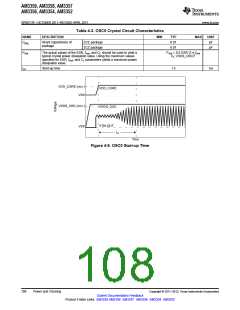
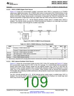
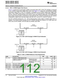
4.2.2.4 OSC1 LVCMOS Digital Clock Source
Figure 4-14 shows the recommended oscillator connections when OSC1 of the ZCE package is connected
to an LVCMOS square-wave digital clock source and Figure 4-15 shows the recommended oscillator
connections when OSC1 of the ZCZ package is connected to an LVCMOS square-wave digital clock
source. The LVCMOS clock source is connected to the RTC_XTALIN terminal. In this mode of operation,
the RTC_XTALOUT terminal should not be used to source any external components. The printed circuit
board design should provide a mechanism to disconnect the RTC_XTALOUT terminal from any external
components or signal traces that may couple noise into OSC1 via the RTC_XTALOUT terminal.
The RTC_XTALIN terminal has a 10 - 40 kΩ internal pull-up resistor which is enabled when OSC1 is
disabled. This internal resistor prevents the RTC_XTALIN terminal from floating to an invalid logic level
which may increase leakage current through the oscillator input buffer.
AM335x
(ZCE Package)
RTC_XTALIN
RTC_XTALOUT
VDDS_RTC
LVCMOS
Digital
Clock
N/C
Source
Figure 4-14. OSC1 (ZCE Package) LVCMOS Circuit Schematic
AM335x
(ZCZ Package)
RTC_XTALIN
VSS_RTC
RTC_XTALOUT
VDDS_RTC
LVCMOS
Digital
Clock
N/C
Source
Figure 4-15. OSC1 (ZCZ Package) LVCMOS Circuit Schematic
Table 4-7. OSC1 LVCMOS Reference Clock Requirements
NAME
DESCRIPTION
MIN
TYP
MAX
UNIT
MHz
ppm
f(RTC_XTALIN)
Frequency, LVCMOS reference clock
32.768
Frequency, LVCMOS reference clock
stability and tolerance(1)
Maximum RTC error =
10.512 minutes/year
-20
-50
20
50
Maximum RTC error = 26.28
minutes/year
ppm
tdc(RTC_XTALIN)
tjpp(RTC_XTALIN)
tR(RTC_XTALIN)
tF(RTC_XTALIN)
Duty cycle, LVCMOS reference clock period
45
-1
55
1
%
%
Jitter peak-to-peak, LVCMOS reference clock period
Time, LVCMOS reference clock rise
5
ns
ns
Time, LVCMOS reference clock fall
5
(1) Initial accuracy, temperature drift, and aging effects should be combined when evaluating a reference clock for this requirement.
112
Power and Clocking
Copyright © 2011–2013, Texas Instruments Incorporated
Submit Documentation Feedback
Product Folder Links: AM3359 AM3358 AM3357 AM3356 AM3354 AM3352

 TI [ TEXAS INSTRUMENTS ]