ADS62P49 / ADS62P29
ADS62P48 / ADS62P28
www.ti.com............................................................................................................................................................. SLAS635A–APRIL 2009–REVISED JUNE 2009
DIGITAL CHARACTERISTICS — ADS62Px9/x8
The DC specifications refer to the condition where the digital outputs are not switching, but are permanently at a valid logic
level 0 or 1. AVDD = 3.3V, DRVDD = 1.8V
ADS62P49/ADS62P48/
ADS62P29/ADS62P28
PARAMETER
TEST CONDITIONS
UNIT
MIN
TYP
MAX
DIGITAL INPUTS – CTRL1, CTRL2, CTRL3, RESET, SCLK, SDATA, SEN(1)
High-level input voltage
Low-level input voltage
1.3
V
V
All digital inputs support 1.8V and 3.3V
CMOS logic levels.
0.4
SDATA, SCLK(2)
SEN(3)
16
10
0
High-level input current
VHIGH = 3.3 V
VLOW = 0 V
µA
SDATA, SCLK
SEN
Low-level input current
Input capacitance
µA
–20
4
pF
DIGITAL OUTPUTS – CMOS INTERFACE (DA0-DA13, DB0-DB13, CLKOUT, SDOUT)
High-level output voltage
IOH = 1mA
DRVDD
–0.1
DRVDD
V
Low-level output voltage
IOL = 1mA
0
2
0.1
V
Output capacitance (internal to device)
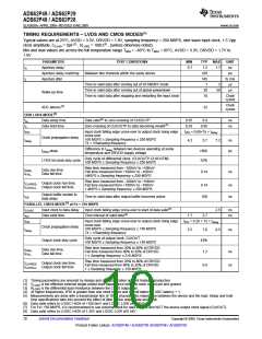
DIGITAL OUTPUTS – LVDS INTERFACE
VODH High-level output differential voltage
VODL Low-level output differential voltage
VOCM Output common-mode voltage
pF
With external 100 Ω termination.
With external 100 Ω termination.
275
–425
1
350
–350
1.15
425
–275
1.4
mV
mV
V
Capacitance inside the device from
each output to ground
Output Capacitance
2
pF
(1) SCLK, SDATA, SEN function as digital input pins in serial configuration mode.
(2) SDATA, SCLK have internal 200 kΩ pull-down resistor
(3) SEN has internal 100 kΩ pull-up resistor to AVDD. Since the pull-up is weak, SEN can also be driven by 1.8V or 3.3V CMOS buffers.
DAnP/DBnP
Dn_Dn+1_P
Logic 0
VODL = –350 mV(1)
Logic 1
VODH = 350 mV(1)
Dn_Dn+1_M
DAnM/DBnM
VOCM
V
GND
GND
T0334-02
(1) With external 100-Ω termination
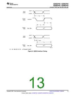
Figure 3. LVDS Output Voltage Levels
Copyright © 2009, Texas Instruments Incorporated
Submit Documentation Feedback
9
Product Folder Link(s): ADS62P49 / ADS62P29 ADS62P48 / ADS62P28

 TI [ TEXAS INSTRUMENTS ]