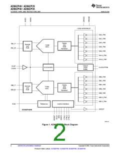
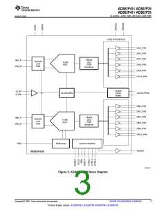
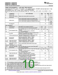
ADS62P49 / ADS62P29
ADS62P48 / ADS62P28
SLAS635A–APRIL 2009–REVISED JUNE 2009............................................................................................................................................................. www.ti.com
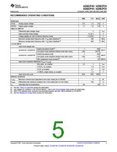
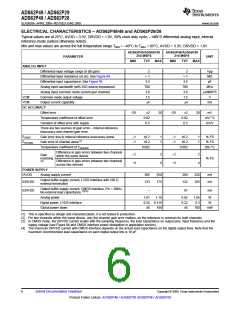
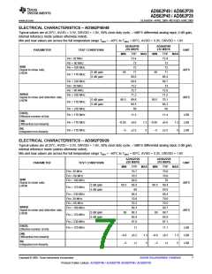
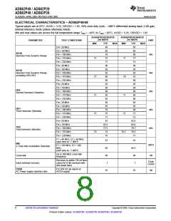
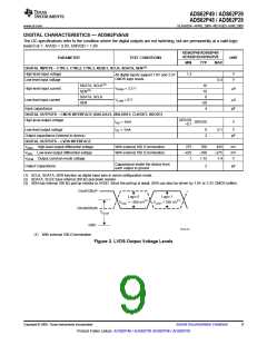
ELECTRICAL CHARACTERISTICS – ADS62P49/48 and ADS62P29/28
Typical values are at 25°C, AVDD = 3.3V, DRVDD = 1.8V, 50% clock duty cycle, –1dBFS differential analog input, internal
reference mode (unless otherwise noted).
Min and max values are across the full temperature range TMIN = –40°C to TMAX = 85°C, AVDD = 3.3V, DRVDD = 1.8V
ADS62P49/ADS62P29
250 MSPS
ADS62P48/ADS62P28
210 MSPS
PARAMETER
UNIT
MIN
TYP
MAX
MIN
TYP
MAX
ANALOG INPUT
Differential input voltage range (0 dB gain)
Differential input resistance (at dc), See Figure 94
Differential input capacitance, See Figure 95
Analog input bandwidth (with 25Ω source impedance)
Analog Input common mode current (per channel)
Common mode output voltage
2
> 1
3.5
700
3.6
1.5
±4
2
> 1
3.5
700
3.6
1.5
±4
Vpp
MΩ
pF
MHz
µA/MSPS
V
VCM
VCM
Output current capability
mA
DC ACCURACY
Offset error
–20
±2
0.02
0.5
20
–20
±2
0.02
0.5
20
mV
Temperature coefficient of offset error
Variation of offset error with supply
mV/ °C
mV/V
There are two sources of gain error – internal reference
inaccuracy and channel gain error.
EGREF
Gain error due to internal reference inaccuracy alone
Gain error of channel alone(1)
–1
–1
±0.2
±0.2
1
1
–1
–1
±0.2
±0.2
1
1
% FS
% FS
EGCHAN
Temperature coefficient of EGCHAN
0.002
0.002
Δ% /°C
Difference in gain errors between two channels
within the same device
–2
–4
2
4
–2
–4
2
4
Gain
matching
% FS
(2)
Difference in gain errors between two channels
across two devices
POWER SUPPLY
IAVDD
Analog supply current
305
133
350
175
280
122
320
165
mA
mA
Output buffer supply current, LVDS interface with 100 Ω
external termination
IDRVDD
Output buffer supply current, CMOS interface, Fin = 2MHz,
No external load capacitance
IDRVDD
–
91
mA
(3)(4)
Analog power
1.01
1.15
0.92
0.22
45
1.05
0.3
W
W
Digital power, LVDS interface
Global power down
0.24 0.315
45 100
100
mW
(1) This is specified by design and characterization; it is not tested in production.
(2) For two channels within the same device, only the channel gain error matters, as the reference is common for both channels.
(3) In CMOS mode, the DRVDD current scales with the sampling frequency, the load capacitance on output pins, input frequency and the
supply voltage (see Figure 86 and CMOS interface power dissipation in application section).
(4) The maximum DRVDD current with CMOS interface depends on the actual load capacitance on the digital output lines. Note that the
maximum recommended load capacitance on each digital output line is 10 pF.
6
Submit Documentation Feedback
Copyright © 2009, Texas Instruments Incorporated
Product Folder Link(s): ADS62P49 / ADS62P29 ADS62P48 / ADS62P28

 TI [ TEXAS INSTRUMENTS ]