ADS62P49 / ADS62P29
ADS62P48 / ADS62P28
www.ti.com............................................................................................................................................................. SLAS635A–APRIL 2009–REVISED JUNE 2009
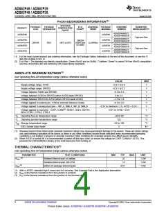
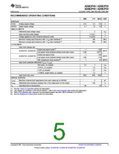
RECOMMENDED OPERATING CONDITIONS
MIN
TYP
MAX UNIT
SUPPLIES
AVDD
Analog supply voltage
3.15
1.7
3.3
1.8
3.6
1.9
V
V
DRVDD Digital supply voltage
ANALOG INPUTS
Differential input voltage range
2
1.5 ±0.1
1.5±0.05
500
VPP
V
Input common-mode voltage
Voltage applied on CM in external reference mode
Maximum analog input frequency with 2 Vpp input amplitude(1)
Maximum analog input frequency with 1 Vpp input amplitude(1)
V
MHz
MHz
800
CLOCK INPUT
Input clock sample rate
Enable low speed mode(2)
1
>100
1
100
250(3)
100
ADS62P49 / ADS62P29
MSPS
MSPS
Low speed mode disabled (default mode after reset)
Enable low speed mode
ADS62P48 / ADS62P28
Low speed mode disabled (default mode after reset)
With multiplexed mode enabled(4)
>100
1
210
65 MSPS
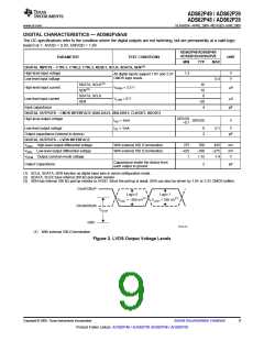
Input clock amplitude differential (VCLKP–VCLKM
)
Sine wave, ac-coupled
LVPECL, ac-coupled
0.2
40%
–40
3
1.6
VPP
VPP
VPP
V
LVDS, ac-coupled
0.7
LVCMOS, single-ended, ac-coupled
3.3
Input clock duty cycle
DIGITAL OUTPUTS
50%
60%
CLOAD
RLOAD
TA
Maximum external load capacitance from each output pin to DRGND
Differential load resistance between the LVDS output pairs (LVDS mode)
Operating free-air temperature
5
pF
Ω
100
85
°C
(1) See the Theory of Operation section for information.
(2) Use register bit <ENABLE LOW SPEED MODE>, refer to the Serial Register Map section for information.
(3) With LVDS interface only; maximum recommended sample rate with CMOS interface is 210 MSPS.
(4) See the Multiplexed Output Mode section for information.
Copyright © 2009, Texas Instruments Incorporated
Submit Documentation Feedback
5
Product Folder Link(s): ADS62P49 / ADS62P29 ADS62P48 / ADS62P28

 TI [ TEXAS INSTRUMENTS ]