ADS62P49 / ADS62P29
ADS62P48 / ADS62P28
SLAS635A–APRIL 2009–REVISED JUNE 2009............................................................................................................................................................. www.ti.com
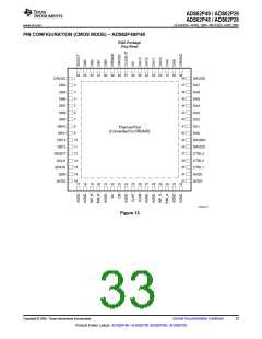
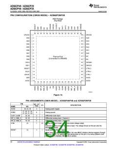
PIN CONFIGURATION (CMOS MODE) – ADS62P29/P28
RGC Package
(Top View)
64 63 62 61 60 59 58 57 56 55 54 53 52 51 50 49
1
48
47
46
45
44
43
42
41
40
39
38
37
36
35
34
33
DRVDD
DB2
DRVDD
DA5
2
3
DB3
DA4
4
DB4
DA3
5
DB5
DA2
6
DB6
DA1
7
DB7
DA0
8
DB8
NC
Thermal Pad
(Connected to DRGND)
9
DB9
NC
10
11
12
13
14
15
16
DB10
DB11
RESET
SCLK
SDATA
SEN
DRGND
DRVDD
CTRL3
CTRL2
CTRL1
AVDD
AVDD
AVDD
17 18 19 20 21 22 23 24 25 26 27 28 29 30 31 32
P0056-17
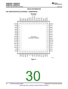
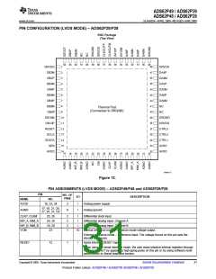
Figure 14.
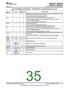
PIN ASSIGNMENTS (CMOS MODE) – ADS62P49/P48 and ADS62P29/P28
PIN
NO. OF
PINS
I/O
DESCRIPTION
NAME
NO.
AVDD
16, 33, 34
3
I
I
Analog power supply
Analog ground
17, 18, 21, 24,
27, 28, 31, I32
AGND
8
CLKP, CLKM
INP_A, INM_A
INP_B, INM_B
VCM
25, 26
29, 30
19, 20
23
2
2
2
1
I
I
I
Differential clock input
Differential analog input, Channel A
Differential analog input, Channel B
IO Internal reference mode – Common-mode voltage output.
External reference mode – Reference input. The voltage forced on this pin sets the
internal references.
RESET
12
1
I
Serial interface RESET input.
When using the serial interface mode, the user MUST initialize internal registers through
hardware RESET by applying a high-going pulse on this pin or by using software reset
option. Refer to SERIAL INTERFACE section.
34
Submit Documentation Feedback
Copyright © 2009, Texas Instruments Incorporated
Product Folder Link(s): ADS62P49 / ADS62P29 ADS62P48 / ADS62P28

 TI [ TEXAS INSTRUMENTS ]