ADS62P49 / ADS62P29
ADS62P48 / ADS62P28
SLAS635A–APRIL 2009–REVISED JUNE 2009............................................................................................................................................................. www.ti.com
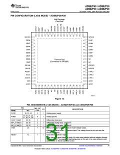
PIN ASSIGNMENTS (LVDS MODE) – ADS62P49/P48 and ADS62P29/P28 (continued)
PIN
NO. OF
PINS
I/O
DESCRIPTION
NAME
NO.
In parallel interface mode, the user has to tie RESET pin permanently high. (SCLK and
SEN are used as parallel control pins in this mode)
The pin has an internal 100 kΩ pull-down resistor.
SCLK
13
1
I
This pin functions as serial interface clock input when RESET is low.
It controls selection of internal or external reference when RESET is tied high. See
Table 4 for detailed information.
The pin has an internal 100 kΩ pull-down resistor.
SDATA
SEN
14
15
1
1
I
I
Serial interface data input.
The pin has an internal 100KΩ pull-down resistor.
It has no function in parallel interface mode and can be tied to ground.
This pin functions as serial interface enable input when RESET is low.
It controls selection of data format and interface type when RESET is tied high. See
Table 5 for detailed information.
The pin has an internal 100 kΩ pull-up resistor to DRVDD
This pin functions as serial interface register readout, when the <SERIAL READOUT> bit
is enabled.
SDOUT
64
1
O
When <SERIAL READOUT> = 0, this pin forces logic LOW and is not 3-stated.
CTRL1
35
36
37
57
56
1
1
1
1
1
2
2
2
2
2
I
CTRL2
I
Digital control input pins. Together, they control various power down modes.
CTRL3
I
CLKOUTP
CLKOUTM
DA0P, DA0M
DA2P, DA2M
DA4P, DA4M
DA6P, DA6M
DA8P, DA8M
O
O
O
O
O
O
O
Differential output clock, true
Differential output clock, complement
Differential output data pair, D0 and D1 multiplexed – Channel A
Differential output data D2 and D3 multiplexed, true – Channel A
Differential output data D4 and D5 multiplexed, true – Channel A
Differential output data D6 and D7 multiplexed, true – Channel A
Differential output data D8 and D9 multiplexed, true – Channel A
DA10P,
DA10M
2
2
O
O
Differential output data D10 and D11 multiplexed, true – Channel A
Differential output data D12 and D13 multiplexed, true – Channel A
DA12P,
DA12M
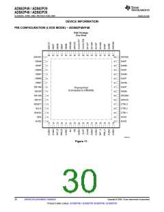
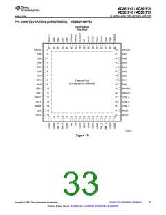
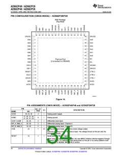
Refer to
Figure 11 and
Figure 12
DB0P, DB0M
DB2P, DB2M
DB4P, DB4M
DB6P, DB6M
DB8P, DB8M
2
2
2
2
2
O
O
O
O
O
Differential output data pair, D0 and D1 multiplexed – Channel B
Differential output data D2 and D3 multiplexed, true – Channel B
Differential output data D4 and D5 multiplexed, true – Channel B
Differential output data D6 and D7 multiplexed, true – Channel B
Differential output data D8 and D9 multiplexed, true – Channel B
DB10P,
DB10M
2
O
Differential output data D10 and D11 multiplexed, true – Channel B
DB12P,
DB12M
2
4
4
O
I
Differential output data D12 and D13 multiplexed, true – Channel B
Output buffer supply
DRVDD
1, 38, 48, 58
39, 49, 59,
PAD
DRGND
I
Output buffer ground
Refer to
Figure 11 and
Figure 12
NC
Do not connect
32
Submit Documentation Feedback
Copyright © 2009, Texas Instruments Incorporated
Product Folder Link(s): ADS62P49 / ADS62P29 ADS62P48 / ADS62P28

 TI [ TEXAS INSTRUMENTS ]