ADS62P49 / ADS62P29
ADS62P48 / ADS62P28
www.ti.com............................................................................................................................................................. SLAS635A–APRIL 2009–REVISED JUNE 2009
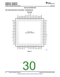
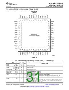
PIN CONFIGURATION (LVDS MODE) – ADS62P29/P28
RGC Package
(Top View)
64 63 62 61 60 59 58 57 56 55 54 53 52 51 50 49
1
48
47
46
45
44
43
42
41
40
39
38
37
36
35
34
33
DRVDD
DB2M
DB2P
DB4M
DB4P
DB6M
DB6P
DB8M
DB8P
DB10M
DB10P
RESET
SCLK
SDATA
SEN
DRVDD
DA4P
DA4M
DA2P
DA2M
DA0P
DA0M
NC
2
3
4
5
6
7
8
Thermal Pad
(Connected to DRGND)
9
NC
10
11
12
13
14
15
16
DRGND
DRVDD
CTRL3
CTRL2
CTRL1
AVDD
AVDD
AVDD
17 18 19 20 21 22 23 24 25 26 27 28 29 30 31 32
P0056-15
Figure 12.
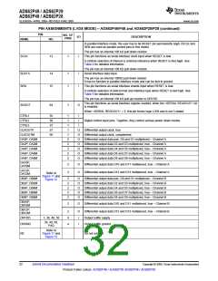
PIN ASSIGNMENTS (LVDS MODE) – ADS62P49/P48 and ADS62P29/P28
PIN
NO. OF
PINS
I/O
DESCRIPTION
NAME
NO.
AVDD
16, 33, 34
3
I
I
Analog power supply
Analog ground
17, 18, 21, 24,
27, 28, 31, I32
AGND
8
CLKP, CLKM
INP_A, INM_A
INP_B, INM_B
VCM
25, 26
29, 30
19, 20
23
2
2
2
1
I
I
I
Differential clock input
Differential analog input, Channel A
Differential analog input, Channel B
IO Internal reference mode – Common-mode voltage output.
External reference mode – Reference input. The voltage forced on this pin sets the
internal references.
RESET
12
1
I
Serial interface RESET input.
When using the serial interface mode, the user must initialize internal registers through
hardware RESET by applying a high-going pulse on this pin or by using software reset
option. Refer to Serial Interface section.
Copyright © 2009, Texas Instruments Incorporated
Submit Documentation Feedback
31
Product Folder Link(s): ADS62P49 / ADS62P29 ADS62P48 / ADS62P28

 TI [ TEXAS INSTRUMENTS ]