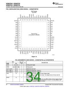
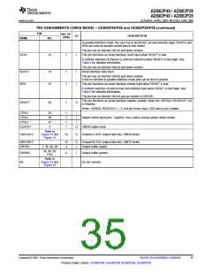
ADS62P49 / ADS62P29
ADS62P48 / ADS62P28
SLAS635A–APRIL 2009–REVISED JUNE 2009............................................................................................................................................................. www.ti.com
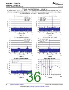
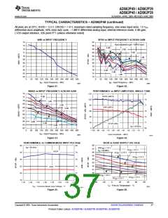
TYPICAL CHARACTERISTICS – ADS62P49 (continued)
All plots are at 25°C, AVDD = 3.3 V, DRVDD = 1.8 V, maximum rated sampling frequency, sine wave input clock. 1.5 VPP
differential clock amplitude, 50% clock duty cycle, –1 dBFS differential analog input, internal reference mode, 0 dB gain,
LVDS output interface, 32K point FFT (unless otherwise noted)
SNR vs AVDD SUPPLY VOLTAGE
AV = 3.2 V
PERFORMANCE vs DRVDD SUPPLY VOLTAGE
72.50
72.25
72.00
71.75
71.50
71.25
71.00
86
85
84
83
82
81
80
79
78
78
AV = 3.3 V
DD
DD
77
76
75
74
73
72
71
70
f
= 60 MHz
IN
AV = 3.4 V
DD
AV = 3.15 V
DD
SFDR
SNR
AV = 3.3 V
DD
AV = 3.6 V
DD
DRV = 1.8 V
DD
f
IN
= 60 MHz
AV = 3.5 V
DD
1.70
1.74
1.78
1.82
1.86
1.90
−40
−20
0
20
40
60
80
T
A
− Free-Air Temperature − °C
DRV − Supply Voltage − V
DD
G013
G014
Figure 27.
Figure 28.
PERFORMANCE vs INPUT CLOCK AMPLITUDE
PERFORMANCE vs INPUT CLOCK DUTY CYCLE
90
88
86
84
82
80
78
76
78
92
90
88
86
84
82
80
78
76
78
f
IN
= 20 MHz
f
IN
= 60 MHz
77
76
75
74
73
72
71
70
77
76
75
74
73
72
71
70
SFDR
SFDR
SNR
SNR
74
0.0
0.5
1.0
1.5
2.0
2.5
30
35
40
45
50
55
60
65
Input Clock Amplitude − V
Input Clock Duty Cycle − %
PP
G015
G016
Figure 29.
Figure 30.
PERFORMANCE IN EXTERNAL REFERENCE MODE
86
84
82
80
78
76
80
f
= 60 MHz
IN
External Reference Mode
78
76
74
72
70
SFDR
SNR
1.30 1.35 1.40 1.45 1.50 1.55 1.60 1.65 1.70
V
VCM
− VCM Voltage − V
G017
Figure 31.
38
Submit Documentation Feedback
Copyright © 2009, Texas Instruments Incorporated
Product Folder Link(s): ADS62P49 / ADS62P29 ADS62P48 / ADS62P28

 TI [ TEXAS INSTRUMENTS ]