ADS131B04-Q1
ZHCSMK3B –NOVEMBER 2020 –REVISED NOVEMBER 2021
www.ti.com.cn
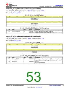
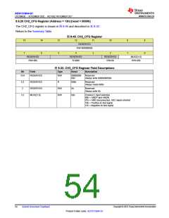
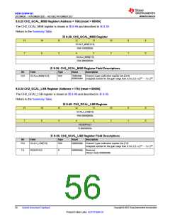
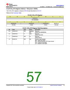
8.6.25 CH3_CFG Register (Address = 18h) [reset = 0000h]
The CH3_CFG register is shown in 图8-50 and described in 表8-37.
Return to the Summary Table.
图8-50. CH3_CFG Register
15
14
13
12
11
10
9
1
8
0
RESERVED
R/W-00000000b
7
6
5
4
3
2
RESERVED
R/W-00b
RESERVED
R-000b
RESERVED
R/W-0b
MUX3[1:0]
R/W-00b
表8-37. CH3_CFG Register Field Descriptions
Bit
Field
Type
Reset
Description
15:6
5:3
2
RESERVED
RESERVED
RESERVED
MUX3[1:0]
R/W
00000000
00b
Reserved
Always write 0000000000b
R
000b
Reserved
Always reads 000b
R/W
R/W
0b
Reserved
Always write 0b
1:0
00b
Channel 3 input selection
00b = AIN3P and AIN3N
01b = AIN3 disconnected, ADC inputs shorted
10b = Positive dc test signal
11b = Negative dc test signal
Copyright © 2022 Texas Instruments Incorporated
Submit Document Feedback
57
Product Folder Links: ADS131B04-Q1

 TI [ TEXAS INSTRUMENTS ]