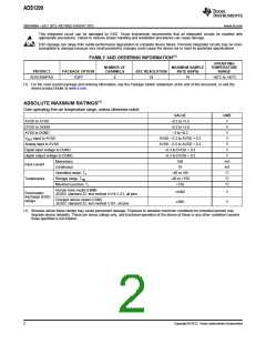
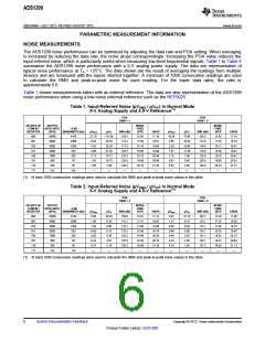
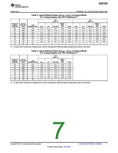
ADS1299
SBAS499A –JULY 2012–REVISED AUGUST 2012
www.ti.com
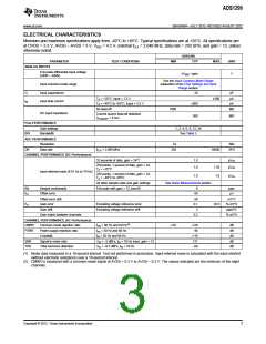
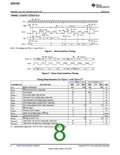
ELECTRICAL CHARACTERISTICS (continued)
Minimum and maximum specifications apply from –40°C to +85°C. Typical specifications are at +25°C. All specifications are
at DVDD = 3.3 V, AVDD – AVSS = 5 V, VREF = 4.5 V, external fCLK = 2.048 MHz, data rate = 250 SPS, and gain = 12, unless
otherwise noted.
ADS1299
PARAMETER
PATIENT BIAS AMPLIFIER
TEST CONDITIONS
MIN
TYP
MAX
UNIT
Integrated noise
BW = 150 Hz
2
100
0.07
–80
μVRMS
kHz
V/μs
dB
GBP
SR
Gain bandwidth product
Slew rate
50 kΩ || 10 pF load, gain = 1
50 kΩ || 10 pF load, gain = 1
fIN = 10 Hz, gain = 1
THD
CMIR
ISC
Total harmonic distortion
Common-mode input range
Short-circuit current
AVSS + 0.3
AVDD – 0.3
V
1.1
20
mA
μA
Quiescent power consumption
LEAD-OFF DETECT
0, fDR / 4
Continuous
Hz
See Register Map section for settings
Frequency
One time or periodic
ILEAD_OFF[1:0] = 00
ILEAD_OFF[1:0] = 01
ILEAD_OFF[1:0] = 10
ILEAD_OFF[1:0] = 11
7.8, 31.2
Hz
nA
nA
μA
μA
%
6
24
Current
6
24
Current accuracy
Comparator threshold accuracy
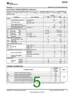
EXTERNAL REFERENCE
±20
±30
mV
VI(ref)
Reference input voltage
Negative input
5-V supply, VREF = (VREFP – VREFN)
4.5
AVSS
V
V
VREFN
VREFP
Positive input
AVSS + 4.5
5.6
V
Input impedance
kΩ
INTERNAL REFERENCE
VO
Output voltage
VREF accuracy
Drift
4.5
±0.2
35
V
%
TA = –40°C to +85°C
ppm
ms
Start-up time
150
SYSTEM MONITORS
Analog supply
Digital supply
2
%
%
Reading error
2
From power-up to DRDY low
STANDBY mode
150
ms
µs
Device wake up
31.25
Voltage
TA = +25°C
145
mV
μV/°C
Hz
Temperature
sensor reading
Coefficient
490
fCLK / 221, fCLK / 220
±1, ±2
Signal frequency
Signal voltage
Accuracy
See Register Map section for settings
See Register Map section for settings
Test signal
mV
%
±2
4
Copyright © 2012, Texas Instruments Incorporated

 TI [ TEXAS INSTRUMENTS ]