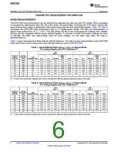
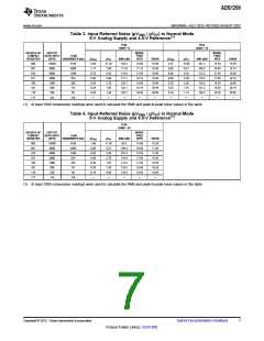
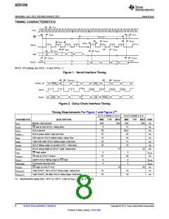
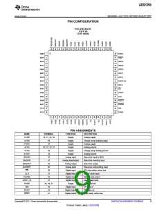
ADS1299
SBAS499A –JULY 2012–REVISED AUGUST 2012
www.ti.com
This integrated circuit can be damaged by ESD. Texas Instruments recommends that all integrated circuits be handled with
appropriate precautions. Failure to observe proper handling and installation procedures can cause damage.
ESD damage can range from subtle performance degradation to complete device failure. Precision integrated circuits may be more
susceptible to damage because very small parametric changes could cause the device not to meet its published specifications.
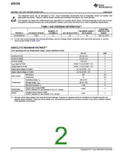
FAMILY AND ORDERING INFORMATION(1)
OPERATING
NUMBER OF
CHANNELS
MAXIMUM SAMPLE
RATE (kSPS)
TEMPERATURE
RANGE
PRODUCT
PACKAGE OPTION
ADC RESOLUTION
ADS1299IPAG
TQFP
8
24
16
–40°C to +85°C
(1) For the most current package and ordering information, see the Package Option Addendum at the end of this document, or visit the
device product folder at www.ti.com.
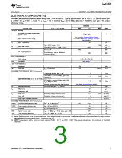
ABSOLUTE MAXIMUM RATINGS(1)
Over operating free-air temperature range, unless otherwise noted.
VALUE
–0.3 to +5.5
UNIT
V
AVDD to AVSS
DVDD to DGND
–0.3 to +3.9
V
AVSS to DGND
–3 to +0.2
V
VREF input to AVSS
Analog input to AVSS
Digital input voltage to DGND
Digital output voltage to DGND
AVSS – 0.3 to AVDD + 0.3
AVSS – 0.3 to AVDD + 0.3
–0.3 to DVDD + 0.3
–0.3 to DVDD + 0.3
100
V
V
V
V
Momentary
Input current
mA
mA
°C
°C
°C
Continuous
10
Operating range, TA
–40 to +85
Temperature
Storage range, Tstg
–60 to +150
Maximum junction, TJ
+150
Human body model (HBM)
JEDEC standard 22, test method A114-C.01, all pins
±1000
±500
V
V
Electrostatic
discharge (ESD)
ratings
Charged device model (CDM)
JEDEC standard 22, test method C101, all pins
(1) Stresses above these ratings may cause permanent damage. Exposure to absolute maximum conditions for extended periods may
degrade device reliability. These are stress ratings only, and functional operation of the device at these or any other conditions beyond
those specified is not implied.
2
Copyright © 2012, Texas Instruments Incorporated

 TI [ TEXAS INSTRUMENTS ]