ADS1299
www.ti.com
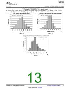
SBAS499A –JULY 2012–REVISED AUGUST 2012
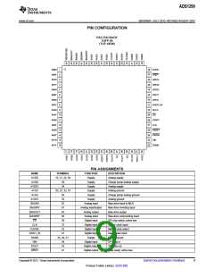
PIN CONFIGURATION
PAG PACKAGE
TQFP-64
(TOP VIEW)
IN8N
IN8P
IN7N
IN7P
IN6N
IN6P
IN5N
IN5P
IN4N
1
2
3
4
5
6
7
8
9
48 DVDD
47 DRDY
46 GPIO4
45 GPIO3
44 GPIO2
43 DOUT
42 GPIO1
41 DAISY_IN
40 SCLK
39 CS
IN4P 10
IN3N 11
IN3P 12
IN2N 13
IN2P 14
IN1N 15
IN1P 16
38 START
37 CLK
36 RESET
35 PWDN
34 DIN
33 DGND
PIN ASSIGNMENTS
NAME
TERMINAL
FUNCTION
DESCRIPTION
AVDD
AVDD
19, 21, 22, 56
Supply
Analog supply
59
Supply
Charge pump analog supply
Analog supply
AVDD1
AVSS
54
Supply
20, 23, 32, 57
Supply
Analog ground
AVSS
58
53
Supply
Charge pump analog ground
Analog ground
AVSS1
BIASIN
BIASINV
BIASOUT
BIASREF
CS
Supply
62
Analog input
Analog input/output
Analog output
Analog input
Digital input
Digital input
Digital input
Digital input
Supply
Bias drive input to MUX
Bias drive inverting input
Bias drive output
61
63
60
Bias drive noninverting input
SPI chip select; active low
Master clock input
Master clock select
Daisy-chain input
39
CLK
37
CLKSEL
DAISY_IN
DGND
DIN
52
41
33, 49, 51
34
Digital ground
Digital input
Digital output
Digital output
SPI data in
DOUT
43
SPI data out
DRDY
47
Data ready; active low
Copyright © 2012, Texas Instruments Incorporated
Submit Documentation Feedback
9
Product Folder Link(s): ADS1299

 TI [ TEXAS INSTRUMENTS ]