excess current dissipation. If the pin is configured as an
output in the DIR register, then the corresponding DIO
register bit value determines the state of the output pin
(0 = GND, 1 = VDD).
serial interface resets on the next SCLK pulse and starts a
new communication cycle. A special pattern on SCLK resets
the entire chip; see the RESET section for additional informa-
tion.
It is still possible to perform A/D conversions on a pin
configured as data I/O. This may be useful as a test mode,
where the data I/O pin is driven and an A/D conversion is
done on the pin.
Data Input (DIN) and Data Output (DOUT)
The data input (DIN) and data output (DOUT) receive and send
data from the ADS1242 and ADS1243. DOUT is high imped-
ance when not in use to allow DIN and DOUT to be connected
together and driven by a bidirectional bus. Note: the Read
Data Continuous Mode (RDATAC) command should not be
issued when DIN and DOUT are connected. While in RDATAC
mode, DIN looks for the STOPC or RESET command. If
either of these 8-bit bytes appear on DOUT (which is con-
nected to DIN), the RDATAC mode ends.
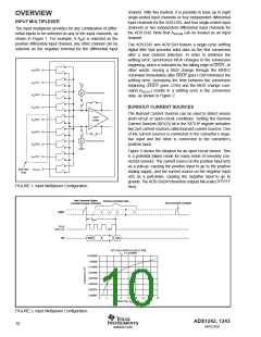
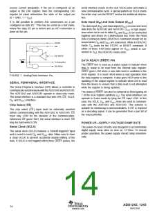
IOCON
DIR
DIO WRITE
AINx/Dx
DATA READY (DRDY) PIN
To Analog Mux
The DRDY line is used as a status signal to indicate when
data is ready to be read from the internal data register.
DRDY goes LOW when a new data word is available in the
DOR register. It is reset HIGH when a read operation from
the data register is complete. It also goes HIGH prior to the
updating of the output register to indicate when not to read
from the device to ensure that a data read is not attempted
while the register is being updated.
DIO READ
FIGURE 7. Analog/Data Interface Pin.
SERIAL PERIPHERAL INTERFACE
The Serial Peripheral Interface (SPI) allows a controller to
communicate synchronously with the ADS1242 and ADS1243.
The ADS1242 and ADS1243 operate in slave-only mode.
The serial interface is a standard four-wire SPI (CS, SCLK,
DIN and DOUT) interface.
The status of DRDY can also be obtained by interrogating bit
7 of the ACR register (address 2H). The serial interface can
operate in 3-wire mode by tying the CS input LOW. In this
case, the SCLK, DIN, and DOUT lines are used to communi-
cate with the ADS1242 and ADS1243. This scheme is
suitable for interfacing to microcontrollers. If CS is required
as a decoding signal, it can be generated from a port bit of
the microcontroller.
Chip Select (CS
)
The chip select (CS) input must be externally asserted
before communicating with the ADS1242 or ADS1243. CS
must stay LOW for the duration of the communication.
Whenever CS goes HIGH, the serial interface is reset. CS
may be hard-wired LOW.
POWER-UP—SUPPLY VOLTAGE RAMP RATE
Serial Clock (SCLK)
The power-on reset circuitry was designed to accommodate
digital supply ramp rates as slow as 1V/10ms. To ensure
proper operation, the power supply should ramp monotoni-
cally.
The serial clock (SCLK) features a Schmitt-triggered input
and is used to clock DIN and DOUT data. Make sure to have
a clean SCLK to prevent accidental double-shifting of the
data. If SCLK is not toggled within three DRDY pulses, the
ADS1242, 1243
14
SBAS235B
www.ti.com

 TI [ TEXAS INSTRUMENTS ]