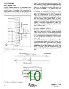
The buffer draws additional current when activated. The
current required by the buffer depends on the PGA setting.
When the PGA is set to 1, the buffer uses approximately
50µA; when the PGA is set to 128, the buffer uses approxi-
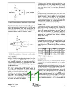
VDD
2µA
mately 500µA.
VDD
PGA
ADC
OPEN CIRCUIT
CODE = 0x7FFFFFH
The Programmable Gain Amplifier (PGA) can be set to gains
of 1, 2, 4, 8, 16, 32, 64, or 128. Using the PGA can improve the
effective resolution of the A/D converter. For instance, with a
PGA of 1 on a 5V full-scale signal, the A/D converter can
resolve down to 1µV. With a PGA of 128 and a full-scale signal
of 39mV, the A/D converter can resolve down to 75nV. VDD
current increases with PGA settings higher than 4.
0V
2µA
FIGURE 3. Burnout detection while sensor is open-circuited.
OFFSET DAC
Figure 4 shows a short-circuited sensor. Since the inputs are
shorted and at the same potential, the ADS1242/43 signal
outputs are approximately zero. (Note that the code for
shorted inputs is not exactly zero due to internal series
resistance, low-level noise and other error sources.)
The input to the PGA can be shifted by half the full-scale input
range of the PGA using the Offset DAC (ODAC) register. The
ODAC register is an 8-bit value; the MSB is the sign and the
seven LSBs provide the magnitude of the offset. Using the
offset DAC does not reduce the performance of the A/D
converter. For more details on the ODAC in the ADS1242/43,
please refer to TI application report SBAA077 (available
through the TI website).
VDD
MODULATOR
2µA
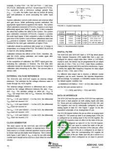
The modulator is a single-loop second-order system. The
modulator runs at a clock speed (fMOD) that is derived from
the external clock (fOSC). The frequency division is deter-
mined by the SPEED bit in the SETUP register, as shown in
Table I.
VDD/2
SHORT
CIRCUIT
ADC
CODE
0
VDD/2
2µA
SPEED
BIT
DR BITS
01
1st NOTCH
FREQ.
fOSC
fMOD
00
10
2.4576MHz
0
1
0
1
19,200Hz 15Hz 7.5Hz 3.75Hz
9,600Hz 7.5Hz 3.75Hz 1.875Hz
50/60Hz
25/30Hz
100/120Hz
50/60Hz
4.9152MHz
38,400Hz 30Hz
15Hz
7.5Hz
FIGURE 4. Burnout detection while sensor is short-circuited.
19,200Hz 15Hz 7.5Hz 3.75Hz
TABLE I. Output Configuration.
INPUT BUFFER
The input impedance of the ADS1242/43 without the buffer
enabled is approximately 5MΩ/PGA. For systems requiring
very high input impedance, the ADS1242/43 provides a
chopper-stabilized differential FET-input voltage buffer. When
activated, the buffer raises the ADS1242/43 input impedance
to approximately 5GΩ.
CALIBRATION
The offset and gain errors can be minimized with calibration.
The ADS1242 and ADS1243 support both self and system
calibration.
Self-calibration of the ADS1242 and ADS1243 corrects inter-
nal offset and gain errors and is handled by three commands:
SELFCAL, SELFGAL, and SELFOCAL. The SELFCAL com-
mand performs both an offset and gain calibration. SELFGCAL
performs a gain calibration and SELFOCAL performs an
offset calibration, each of which takes two tDATA periods to
complete. During self-calibration, the ADC inputs are discon-
nected internally from the input pins. The PGA must be set to
1 prior to issuing a SELFCAL or SELFGCAL command. Any
PGA is allowed when issuing a SELFOCAL command. For
The buffer’s input range is approximately 50mV to
VDD – 1.5V. The buffer’s linearity will degrade beyond this
range. Differential signals should be adjusted so that both
signals are within the buffer’s input range.
The buffer can be enabled using the BUFEN pin or the
BUFEN bit in the ACR register. The buffer is on when the
BUFEN pin is high and the BUFEN bit is set to one. If the
BUFEN pin is low, the buffer is disabled. If the BUFEN bit is
set to zero, the buffer is also disabled.
ADS1242, 1243
11
SBAS235B
www.ti.com

 TI [ TEXAS INSTRUMENTS ]