example, if using PGA = 64, first set PGA = 1 and issue
SELFGCAL. Afterwards, set PGA = 64 and issue SELFOCAL.
For operation with a reference voltage greater than
(VDD – 1.5) volts, the buffer must also be turned off during
gain self-calibration to avoid exceeding the buffer input
range.
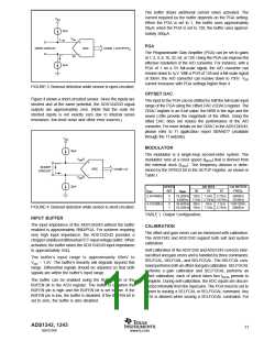
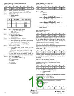
XIN
C1
C2
Crystal
XOUT
System calibration corrects both internal and external offset
and gain errors. While performing system calibration, the
appropriate signal must be applied to the inputs. The system
offset calibration command (SYSOCAL) requires a zero input
differential signal (see Table IV, page 18). It then computes
the offset that nullifies the offset in the system. The system
gain calibration command (SYSGCAL) requires a positive
full-scale input signal. It then computes a value to nullify the
gain error in the system. Each of these calibrations takes two
FIGURE 5. Crystal Connection.
CLOCK
PART
NUMBER
SOURCE FREQUENCY
C1
C2
Crystal
Crystal
Crystal
Crystal
2.4576
4.9152
4.9152
4.9152
0-20pF 0-20pF ECS, ECSD 2.45 - 32
0-20pF 0-20pF
0-20pF 0-20pF
ECS, ECSL 4.91
ECS, ECSD 4.91
t
DATA periods to complete. System gain calibration is recom-
0-20pF 0-20pF CTS, MP 042 4M9182
mended for the best gain calibration at higher PGAs.
Calibration should be performed after power on, a change in
temperature, or a change of the PGA. The RANGE bit (ACR bit
2) must be zero during calibration.
TABLE II. Recommended Crystals.
DIGITAL FILTER
Calibration removes the effects of the ODAC; therefore, dis-
able the ODAC during calibration, and enable again after
calibration is complete.
The ADS1242 and ADS1243 have a 1279 tap linear phase
Finite Impulse Response (FIR) digital filter that a user can
configure for various output data rates. When a 2.4576MHz
crystal is used, the device can be programmed for an output
data rate of 15Hz, 7.5Hz, or 3.75Hz. Under these conditions,
the digital filter rejects both 50Hz and 60Hz interference. Figure
6 shows the digital filter frequency response for data output
rates of 15Hz, 7.5Hz, and 3.75Hz.
At the completion of calibration, the DRDY signal goes low,
indicating the calibration is finished. The first data after
calibration should be discarded since it may be corrupt from
calibration data remaining in the filter. The second data is
always valid.
If a different data output rate is desired, a different crystal
frequency can be used. However, the rejection frequencies
shift accordingly. For example, a 3.6864MHz master clock with
the default register condition has:
EXTERNAL VOLTAGE REFERENCE
The ADS1242 and ADS1243 require an external voltage
reference. The selection for the voltage reference value is
made through the ACR register.
(3.6864MHz/2.4576MHz) • 15Hz = 22.5Hz data output rate
and the first and second notch is:
The external voltage reference is differential and is repre-
sented by the voltage difference between the pins: +VREF
and –VREF. The absolute voltage on either pin, +VREF or
–VREF, can range from GND to VDD. However, the following
limitations apply:
1.5 • (50Hz and 60Hz) = 75Hz and 90Hz
DATA I/O INTERFACE
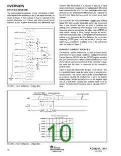
The ADS1242 has four pins and the ADS1243 has eight pins
that serve a dual purpose as both analog inputs and data
I/O. These pins are configured through the IOCON, DIR, and
DIO registers and can be individually configured as either
analog inputs or data I/O. See Figure 7 (page 14) for the
equivalent schematic of an Analog/Data I/O pin.
For VDD = 5.0V and RANGE = 0 in the ACR, the differential
V
REF must not exceed 2.5V.
For VDD = 5.0V and RANGE = 1 in the ACR, the differential
REF must not exceed 5V.
For VDD = 3.0V and RANGE = 0 in the ACR, the differential
REF must not exceed 1.25V.
V
V
The IOCON register defines the pin as either an analog input
or data I/O. The power-up state is an analog input. If the pin
is configured as an analog input in the IOCON register, the
DIR and DIO registers have no effect on the state of the pin.
For VDD = 3.0V and RANGE = 1 in the ACR, the differential
VREF must not exceed 2.5V.
CLOCK GENERATOR
If the pin is configured as data I/O in the IOCON register,
then DIR and DIO are used to control the state of the pin.
The DIR register controls the direction of the data pin, either
as an input or output. If the pin is configured as an input in
the DIR register, then the corresponding DIO register bit
reflects the state of the pin. Make sure the pin is driven to a
logic one or zero when configured as an input to prevent
The clock source for the ADS1242 and ADS1243 can be
provided from a crystal, oscillator, or external clock. When the
clock source is a crystal, external capacitors must be provided
to ensure start-up and stable clock frequency. This is shown in
both Figure 5 and Table II. XOUT is only for use with external
crystals and it should not be used as a clock driver for external
circuitry.
ADS1242, 1243
12
SBAS235B
www.ti.com

 TI [ TEXAS INSTRUMENTS ]