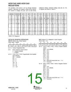
ACR (Address 02H) Analog Control Register
ODAC (Address 03 ) Offset DAC
Reset Value = X0H
Reset Value = 00H
bit 7
bit 6
bit 5
bit 4
bit 3
bit 2
bit 1
DR1
bit 0
DR0
bit 7
bit 6
bit 5
bit 4
bit 3
bit 2
bit 1
bit 0
DRDY
U/B
SPEED
BUFEN BIT ORDER RANGE
SIGN
OSET6
OSET5
OSET4
OSET3
OSET2
OSET1
OSET0
bit 7
DRDY: Data Ready (Read Only)
This bit duplicates the state of the DRDY pin.
U/ : Data Format
bit 7
Sign
0 = Positive
1 = Negative
bit 6
B
0 = Bipolar (default)
1 = Unipolar
VREF
OSET[6 : 0]
127
Offset =
•
RANGE = 0
RANGE = 1
2 • PGA
U/B
ANALOG INPUT
DIGITAL OUTPUT (Hex)
+FSR
Zero
0x7FFFFF
0x000000
0x800000
0xFFFFFF
0x000000
0x000000
VREF
OSET[6 : 0]
127
0
Offset =
•
4 • PGA
–FSR
+FSR
Zero
1
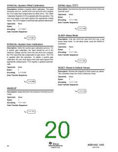
NOTE: The offset DAC must be enabled after calibration or the calibration
nullifies the effects.
–FSR
bit 5
bit 4
bit 3
SPEED: Modulator Clock Speed
0 = fMOD = fOSC/128 (default)
1 = fMOD = fOSC/256
DIO (Address 04H) Data I/O
Reset Value = 00H
bit 7
bit 6
bit 5
bit 4
bit 3
bit 2
bit 1
bit 0
BUFEN: Buffer Enable
0 = Buffer Disabled (default)
1 = Buffer Enabled
DIO 7
DIO 6
DIO 5
DIO 4
DIO 3
DIO 2
DIO 1
DIO 0
If the IOCON register is configured for data, a value written
to this register appears on the data I/O pins if the pin is
configured as an output in the DIR register. Reading this
register returns the value of the data I/O pins.
BIT ORDER: Data Output Bit Order
0 = Most Significant Bit Transmitted First (default)
1 = Least Significant Bit Transmitted First
Data is always shifted in or out MSB first.
Bits 4 to 7 are not used in ADS1242.
bit 2
RANGE: Range Select
0 = Full-Scale Input Range equal to ±VREF
(default).
DIR (Address 05H) Direction Control for Data I/O
Reset Value = FFH
1 = Full-Scale Input Range equal to ±1/2 VREF
bit 7
bit 6
bit 5
bit 4
bit 3
bit 2
bit 1
bit 0
NOTE: This allows reference voltages as high as
DIR7
DIR6
DIR5
DIR4
DIR3
DIR2
DIR1
DIR0
V
DD, but even with a 5V reference voltage the
calibration must be performed with this bit set to 0.
bit 1-0 DR1: DR0: Data Rate
(fOSC = 2.4576MHz, SPEED = 0)
Each bit controls whether the corresponding data I/O pin is
an output (= 0) or input (= 1). The default power-up state is
as inputs.
00 = 15Hz (default)
01 = 7.5Hz
Bits 4 to 7 are not used in ADS1242.
10 = 3.75Hz
IOCON (Address 06H) I/O Configuration Register
11 = Reserved
Reset Value = 00H
bit 7
bit 6
bit 5
bit 4
IO4
bit 3
IO3
bit 2
IO2
bit 1
IO1
bit 0
IO0
IO7
IO6
IO5
bit 7-0 IO7: IO0: Data I/O Configuration
0 = Analog (default)
1 = Data
Configuring the pin as a data I/O pin allows it to be controlled
through the DIO and DIR registers.
Bits 4 to 7 are not used in ADS1242.
OCR0 (Address 07H) Offset Calibration Coefficient
(Least Significant Byte)
Reset Value = 00H
bit 7
bit 6
bit 5
bit 4
bit 3
bit 2
bit 1
bit 0
OCR07
OCR06
OCR05
OCR04
OCR03
OCR02
OCR01
OCR00
ADS1242, 1243
16
SBAS235B
www.ti.com

 TI [ TEXAS INSTRUMENTS ]