channel. With this method, it is possible to have up to eight
single-ended input channels or four independent differential
input channels for the ADS1243, and four single-ended input
channels or two independent differential input channels for
the ADS1242. Note that AINCOM can be treated as an input
channel.
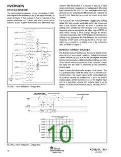
OVERVIEW
INPUT MULTIPLEXER
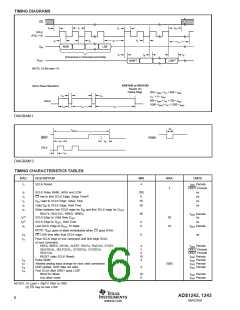
The input multiplexer provides for any combination of differ-
ential inputs to be selected on any of the input channels, as
shown in Figure 1. For example, if AIN0 is selected as the
positive differential input channel, any other channel can be
selected as the negative terminal for the differential input
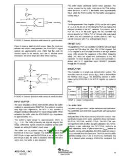
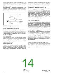
The ADS1242 and ADS1243 feature a single-cycle settling
digital filter that provides valid data on the first conversion
after a new channel selection. In order to minimize the
settling error, synchronize MUX changes to the conversion
beginning, which is indicated by the falling edge of DRDY. In
other words, issuing a MUX change through the WREG
command immediately after DRDY goes LOW minimizes the
settling error. Increasing the time between the conversion
beginning (DRDY goes LOW) and the MUX change com-
mand (tDELAY) results in a settling error in the conversion
data, as shown in Figure 2.
A
A
IN0/D0
IN1/D1
VDD
Burnout Current Source
AIN2/D2
AIN3/D3
AIN4/D4
AIN5/D5
AIN6/D6
AIN7/D7
AINCOM
BURNOUT CURRENT SOURCES
The Burnout Current Sources can be used to detect sensor
short-circuit or open-circuit conditions. Setting the Burnout
Current Sources (BOCS) bit in the SETUP register activates
two 2µA current sources called burnout current sources. One
of the current sources is connected to the converter’s nega-
tive input and the other is connected to the converter’s
positive input.
Input
Buffer
Burnout Current Source
GND
Figure 3 shows the situation for an open-circuit sensor. This
is a potential failure mode for many kinds of remotely con-
nected sensors. The current source on the positive input acts
as a pull-up, causing the positive input to go to the positive
analog supply, and the current source on the negative input
acts as a pull-down, causing the negative input to go to
ground. The ADS1242/43 therefore outputs full-scale (7FFFFF
Hex).
ADS1243
Only
FIGURE 1. Input Multiplexer Configuration.
New Conversion Begins,
Complete Previous Conversion
Previous Conversion Data
New Conversion Complete
DRDY
tDELAY
SCLK
(POL = 0)
DIN
MSB
LSB
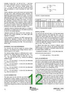
SETTLING ERROR vs DELAY TIME
CLK = 2.4576MHz
f
10.000000
1.000000
0.100000
0.010000
0.001000
0.000100
0.000010
0.000001
0
2
4
6
8
10
12
14
16
Delay Time, tDELAY (ms)
FIGURE 2. Input Multiplexer Configuration.
10
ADS1242, 1243
SBAS235B
www.ti.com

 TI [ TEXAS INSTRUMENTS ]