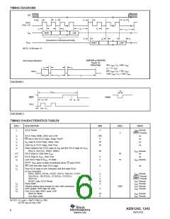
TIMING DIAGRAMS
CS
t3
t1
t2
t10
SCLK
(POL = 0)
t2
t4
t5
t6
t11
DIN
MSB
LSB
t7
t8
t9
(Command or Command and Data)
MSB(1)
LSB(1)
DOUT
NOTE: (1) Bit order = 0.
ADS1242 or ADS1243
Resets On
SCLK Reset Waveform
Falling Edge
300 • tOSC < t12 < 500 • tOSC
t13 : > 5 • tOSC
t13
t13
550 • tOSC < t14 < 750 • tOSC
SCLK
1050 • tOSC < t15 < 1250 • tOSC
t12
t14
t15
DIAGRAM 1.
t16
tDATA
DRDY
SCLK
PDWN
t17
t18
t19
DIAGRAM 2.
TIMING CHARACTERISTICS TABLES
SPEC
DESCRIPTION
MIN
MAX
UNITS
t1
SCLK Period
4
tOSC Periods
3
DRDY Periods
t2
t3
t4
t5
t6
SCLK Pulse Width, HIGH and LOW
CS low to first SCLK Edge; Setup Time(2)
DIN Valid to SCLK Edge; Setup Time
Valid DIN to SCLK Edge; Hold Time
200
0
ns
ns
ns
ns
50
50
Delay between last SCLK edge for DIN and first SCLK edge for DOUT
:
RDATA, RDATAC, RREG, WREG
SCLK Edge to Valid New DOUT
50
tOSC Periods
ns
(1)
t7
50
10
(1)
t8
SCLK Edge to DOUT, Hold Time
0
6
ns
t9
Last SCLK Edge to DOUT Tri-State
tOSC Periods
NOTE: DOUT goes tri-state immediately when CS goes HIGH.
CS LOW time after final SCLK edge.
t10
t11
0
ns
Final SCLK edge of one command until first edge SCLK
of next command:
RREG, WREG, DSYNC, SLEEP, RDATA, RDATAC, STOPC
SELFGCAL, SELFOCAL, SYSOCAL, SYSGCAL
SELFCAL
4
2
4
16
4
tOSC Periods
DRDY Periods
DRDY Periods
tOSC Periods
tOSC Periods
tOSC Periods
tOSC Periods
RESET (also SCLK Reset)
t16
t17
t18
t19
Pulse Width
Allowed analog input change for next valid conversion.
DOR update, DOR data not valid.
First SCLK after DRDY goes LOW:
RDATAC Mode
5000
4
10
0
tOSC Periods
tOSC Periods
Any other mode
NOTES: (1) Load = 20pF 10kΩ to GND.
(2) CS may be tied LOW.
ADS1242, 1243
6
SBAS235B
www.ti.com

 TI [ TEXAS INSTRUMENTS ]