71M6521BE
Energy Meter IC
DATA SHEET
JANUARY 2008
OPT_FDC[1:0]
OPT_RXDIS
2007[1:0]
2008[5]
0
0
0
0
R/W Selects OPT_TX modulation duty cycle
OPT_FDC
Function
00
01
10
11
50% Low
25% Low
12.5% Low
6.25% Low
R/W OPT_RX can be configured as an analog input to the optical UART
comparator or as a digital input/output, DIO1.
0—OPT_RX, 1—DIO1.
OPT_RXINV
2008[4]
0
0
R/W Inverts result from OPT_RX comparator when 1. Affects only the
UART input. Has no effect when OPT_RX is used as a DIO input.
R/W Configures the OPT_TX output pin.
OPT_TXE[1,0]
2007[7,6]
00
00
00—OPT_TX, 01—DIO2, 10—WPULSE, 11—RESERVED
R/W Invert OPT_TX when 1. This inversion occurs before modulation.
R/W Enables modulation of OPT_TX. When OPT_TXMOD is set,
OPT_TX is modulated when it would otherwise have been zero.
The modulation is applied after any inversion caused by
OPT_TXINV.
OPT_TXINV
OPT_TXMOD
2008[0]
2008[1]
0
0
0
0
PLL_OK
2003[6]
0
0
R
Indicates that system power is present and the clock generation PLL
is settled.
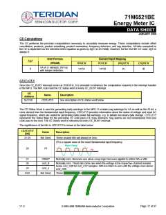
PLS_MAXWIDTH
[7:0]
2080[7:0]
FF
FF
R/W Determines the maximum width of the pulse (low going pulse).
Maximum pulse width is (2*PLS_MAXWIDTH + 1)*TI. Where TI is
PLS_INTERVAL. If PLS_INTERVAL=0, TI is the sample time
(397µs). If 255, disable MAXWIDTH.
PLS_INTERVAL
[7:0]
2081[7:0]
2004[6]
0
0
0
0
R/W If the FIFO is used, PLS_INTERVAL must be set to 81. If
PLS_INTERVAL = 0, the FIFO is not used and pulses are output as
soon as the CE issues them.
R/W Inverts the polarity of WPULSE. Normally, these pulses are active
low. When inverted, they become active high.
PLS_INV
PREBOOT
SFRB2[7]
2001[7:6]
2002[3]
--
0
0
--
0
0
R
Indicates that preboot sequence is active.
The duration of the pre-summer, in samples.
00-42, 01-50, 10-84, 11-100.
PRE_SAMPS[1:0]
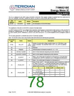
RTM_E
R/W
R/W Real Time Monitor enable. When ‘0’, the RTM output is low. This bit
enables the two wire version of RTM
RTM0[7:0]
RTM1[7:0]
RTM2[7:0]
RTM3[7:0]
SECURE
2060
2061
2062
2063
0
0
0
0
0
0
0
0
0
0
0
--
0
0
R/W Four RTM probes. Before each CE code pass, the values of these
registers are serially output on the RTM pin. The RTM registers are
ignored when RTM_E=0.
SFRB2[6]
R/W Enables security provisions that prevent external reading of flash
memory and CE program RAM. This bit is reset on chip reset and
may only be set. Attempts to write zero are ignored.
SLEEP
20A9[6]
W
Takes the 6521BE to sleep mode. Ignored if system power is
present. The 6521BE will wake when the autowake timer times out,
when push button is pushed, or when system power returns.
SUM_CYCLES[5:0]
2001[5:0]
R/W The number of pre-summer outputs summed in the final summer.
Page: 74 of 97
© 2005-2008 TERIDIAN Semiconductor Corporation
V1.0

 TERIDIAN [ TERIDIAN SEMICONDUCTOR CORPORATION ]