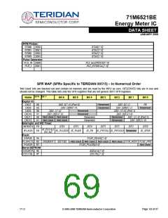
71M6521BE
Energy Meter IC
DATA SHEET
JANUARY 2008
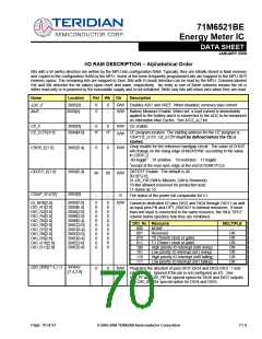
INTBITS
SFRF8[6:0]
--
0
0
--
--
--
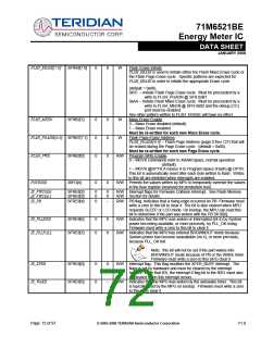
R/W Interrupt inputs. The MPU may read these bits to see the input to
external interrupts INT0, INT1, up to INT6. These bits do not have
any memory and are primarily intended for debug use.
R/W Identifies which segments connected to SEG18 and SEG19 should
blink. 1 means ‘blink.’ Most significant bit corresponds to COM3.
Least significant, to COM0.
LCD_BLKMAP19[3:0]
LCD_BLKMAP18[3:0]
205A[7:4]
205A[3:0]
LCD_CLK[1:0]
2021[1:0]
R/W Sets the LCD clock frequency (for COM/SEG pins, not frame rate).
Note: fw = 32768Hz
00: fw/29, 01: fw/28, 10: fw/27, 11: fw/26
LCD_E
2021[5]
0
0
--
--
R/W Enables the LCD display. When disabled, VLC2, VLC1, and VLC0
are ground as are the COM and SEG outputs.
R/W The LCD bias mode.
LCD_MODE[2:0]
2021[4:2]
000: 4 states, 1/3 bias
001: 3 states, 1/3 bias
010: 2 states, ½ bias
011: 3 states, ½ bias
100: static display
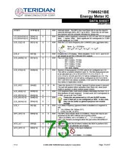
LCD_NUM[4:0]
2020[4:0]
0
0
--
0
R/W Number of dual-purpose LCD/DIO pins to be configured as LCD.
This will be a number between 0 and 18. The first dual-purpose pin
to be allocated as LCD is SEG37/DIO17 if LCD_NUM=5. If
LCD_NUM=6, SEG36 and SEG 37 will be configured as LCD. The
remaining SEG35 to SEG24 will be configured as DIO16 to DIO4.
DIO1 and DIO2 are always available, if not used for the optical port.
See tables in Application Section.
LCD_ONLY
20A9[5]
W
Takes the device to LCD mode. Ignored if system power is present.
The part will awaken when autowake timer times out, when push
button is pushed, or when system power returns.
LCD_SEG0[3:0]
…
LCD_SEG19[3:0]
LCD_SEG24[3:0]
…
2030[3:0]
…
2043[3:0]
2048[3:0]
…
0
…
0
0
…
0
--
…
--
--
…
--
R/W LCD Segment Data. Each word contains information for from 1 to 4
time divisions of each segment. In each word, bit 0 corresponds to
COM0, on up to bit 3 for COM3.
These bits are preserved in LCD and SLEEP modes,
even if their pin is not configured as SEG. In this case,
they can be useful as general-purpose non-volatile
storage.
R/W
2056[3:0]
LCD_SEG38[3:0]
LCD_Y
2021[6]
0
0
0
0
R/W LCD Blink Frequency (ignored if blink is disabled or if segment is
off).
0: 1Hz (500ms ON, 500ms OFF)
1: 0.5Hz (1s ON, 1s OFF)
MPU_DIV[2:0]
2004[2:0]
R/W The MPU clock divider (from 4.9152MHz). These bits may be pro-
grammed by the MPU without risk of losing control.
000-4.9152MHz, 001-4.9152MHz /21, …, 111-4.9152MHz /27
MPU_DIV remains unchanged when the part enters BROWNOUT
mode.
MUX_ALT
2005[2]
0
0
0
0
R/W The MPU asserts this bit when it wishes the MUX to perform ADC
conversions on an alternate set of inputs.
R/W The number of states in the input multiplexer.
MUX_DIV[1:0]
2002[7:6]
00- illegal
01- 4 states 10-3 states 11-2 states
V1.0
© 2005-2008 TERIDIAN Semiconductor Corporation
Page: 73 of 97

 TERIDIAN [ TERIDIAN SEMICONDUCTOR CORPORATION ]