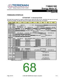
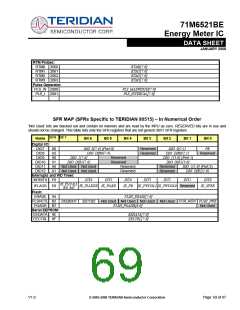
71M6521BE
Energy Meter IC
DATA SHEET
JANUARY 2008
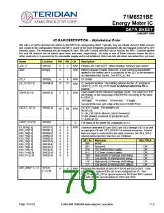
FLSH_ERASE[7:0]
SFR94[7:0]
0
0
W
Flash Erase Initiate
FLSH_ERASE is used to initiate either the Flash Mass Erase cycle or
the Flash Page Erase cycle. Specific patterns are expected for
FLSH_ERASE in order to initiate the appropriate Erase cycle.
(default = 0x00).
0x55 – Initiate Flash Page Erase cycle. Must be proceeded by a
write to FLSH_PGADR @ SFR 0xB7.
0xAA – Initiate Flash Mass Erase cycle. Must be proceeded by a
write to FLSH_MEEN @ SFR 0xB2 and the debug (CC)
port must be enabled.
Any other pattern written to FLSH_ERASE will have no effect.
FLSH_MEEN
SFRB2[1]
0
0
0
0
0
0
W
W
Mass Erase Enable
0 – Mass Erase disabled (default).
1 – Mass Erase enabled.
Must be re-written for each new Mass Erase cycle.
FLSH_PGADR[6:0] SFRB7[7:1]
Flash Page Erase Address
FLSH_PGADR[6:0] – Flash Page Address (page 0 thru 127) that will
be erased during the Page Erase cycle. (default = 0x00).
Must be re-written for each new Page Erase cycle.
FLSH_PWE
SFRB2[0]
R/W Program Write Enable
0 – MOVX commands refer to XRAM Space, normal operation
(default).
1 – MOVX @DPTR,A moves A to Program Space (Flash) @ DPTR.
This bit is automatically reset after each byte written to flash. Writes
to this bit are inhibited when interrupts are enabled.
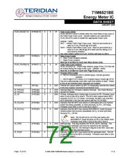
FOVRIDE
20FD[4]
0
0
R/W Permits the values written by MPU to temporarily override the values
in the fuse register (reserved for production test).
IE_FWCOL0
IE_FWCOL1
IE_PB
SFRE8[2]
SFRE8[3]
SFRE8[4]
0
0
0
0
0
--
R/W Interrupt flags for Firmware Collision Interrupt. See Flash Memory
R/W Section for details.
R/W PB flag. Indicates that a rising edge occurred on PB. Firmware must
write a zero to this bit to clear it. The bit is also cleared when MPU
requests SLEEP or LCD mode. On bootup, the MPU can read this
bit to determine if the part was woken with the PB DIO0[0].
R/W Indicates that the MPU was woken or interrupted (int 4) by System
power becoming available, or more precisely, by PLL_OK rising.
Firmware must write a zero to this bit to clear it
R/W Indicates that the MPU has entered BROWNOUT mode because
System power has become unavailable (int 4), or more precisely,
because PLL_OK fell.
IE_PLLRISE
IE_PLLFALL
SFRE8[6]
SFRE8[7]
0
0
0
0
Note: this bit will not be set if the part wakes into
BROWNOUT mode because of PB or the WAKE timer.
Firmware must write a zero to this bit to clear it.
IE_XFER
IE_WAKE
SFRE8[0]
SFRE8[5]
0
0
0
R/W Interrupt flag. This flag monitors the XFER_BUSY interrupt. The
flags is set by hardware and must be cleared by the interrupt
handler. Note that IE6, the interrupt 6 flag bit in the 8051 must also
be cleared when this interrupt occurs.
R/W Indicates that the MPU was woken by the autowake timer. This bit
is typically read by the MPU on bootup. Firmware must write a zero
to this bit to clear it
--
Page: 72 of 97
© 2005-2008 TERIDIAN Semiconductor Corporation
V1.0

 TERIDIAN [ TERIDIAN SEMICONDUCTOR CORPORATION ]