TSC80C31/80C51
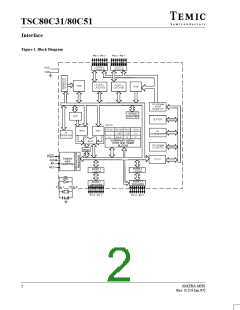
Pin Description
It also receives the high-order address bits and control
signals during program verification in the
TSC80C31/80C51. Port 2 can sink or source three LS
TTL inputs. It can drive CMOS inputs without external
pullups.
VSS
Circuit ground potential.
VCC
Supply voltage during normal, Idle, and Power Down
operation.
Port 3
Port 3 is an 8 bit bi-directional I/O port with internal
pullups. Port 3 pins that have 1’s written to them are
pulled high by the internal pullups, and in that state can
be used as inputs. As inputs, Port 3 pins that are externally
being pulled low will source current (ILL, on the data
sheet) because of the pullups. It also serves the functions
of various special features of the TEMIC C51 Family, as
listed below.
Port 0
Port 0 is an 8 bit open drain bi-directional I/O port. Port 0
pins that have 1’s written to them float, and in that state
can be used as high-impedance inputs.
Port 0 is also the multiplexed low-order address and data
bus during accesses to external Program and Data
Memory. In this application it uses strong internal pullups
when emitting 1’s. Port 0 also outputs the code bytes
during program verification in the TSC80C31/80C51.
External pullups are required during program
verification. Port 0 can sink eight LS TTL inputs.
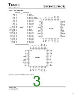
Port Pin
Alternate Function
P3.0
P3.1
P3.2
P3.3
P3.4
P3.5
P3.6
P3.7
RXD (serial input port)
TXD (serial output port)
INT0 (external interrupt 0)
INT1 (external interrupt 1)
TD (Timer 0 external input)
T1 (Timer 1 external input)
WR (external Data Memory write strobe)
RD (external Data Memory read strobe)
Port 1
Port 1 is an 8 bit bi-directional I/O port with internal Port 3 can sink or source three LS TTL inputs. It can drive
pullups. Port 1 pins that have 1’s written to them are CMOS inputs without external pullups.
pulled high by the internal pullups, and in that state can
be used as inputs. As inputs, Port 1 pins that are externally
being pulled low will source current (IIL, on the data
RST
A high level on this for two machine cycles while the
oscillator is running resets the device. An internal
pull-down resistor permits Power-On reset using only a
sheet) because of the internal pullups.
Port 1 also receives the low-order address byte during
program verification. In the TSC80C31/80C51, Port 1
can sink or source three LS TTL inputs. It can drive
CMOS inputs without external pullups.
capacitor connected to V . As soon as the Reset is
CC
applied (Vin), PORT 1, 2 and 3 are tied to one. This
operation is achieved asynchronously even if the
oscillator does not start-up.
Port 2
ALE
Port 2 is an 8 bit bi-directional I/O port with internal
pullups. Port 2 pins that have 1’s written to them are Address Latch Enable output for latching the low byte of
pulled high by the internal pullups, and in that state can the address during accesses to external memory. ALE is
be used as inputs. As inputs, Port 2 pins that are externally activated as though for this purpose at a constant rate of
being pulled low will source current (ILL, on the data 1/6 the oscillator frequency except during an external
sheet) because of the internal pullups. Port 2 emits the data memory access at which time one ALE pulse is
high-order address byte during fetches from external skipped. ALE can sink/source 8 LS TTL inputs. It can
Program Memory and during accesses to external Data drive CMOS inputs without an external pullup.
Memory that use 16 bit addresses (MOVX @DPTR). In If desired, ALE operation can be disabled by setting bit
this application, it uses strong internal pullups when 0 of SFR location AFh (MSCON). With the bit set, ALE
emitting 1’s. During accesses to external Data Memory is active only during MOVX instruction and external
that use 8 bit addresses (MOVX @Ri), Port 2 emits the fetches. Otherwise the pin is pulled low. MSCON SFR is
contents of the P2 Special Function Register.
set to XXXXXXX0 by reset.
4
MATRA MHS
Rev. E (14 Jan.97)

 TEMIC [ TEMIC SEMICONDUCTORS ]