AN1001
AN1001
Fundamental Characteristics of Thyristors
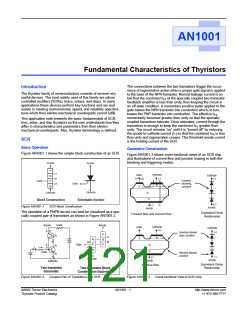
The connections between the two transistors trigger the occur-
rence of regenerative action when a proper gate signal is applied
Introduction
The thyristor family of semiconductors consists of several very
useful devices. The most widely used of this family are silicon
controlled rectifiers (SCRs), triacs, sidacs, and diacs. In many
applications these devices perform key functions and are real
assets in meeting environmental, speed, and reliability specifica-
tions which their electro-mechanical counterparts cannot fulfill.
This application note presents the basic fundamentals of SCR,
triac, sidac, and diac thyristors so the user understands how they
differ in characteristics and parameters from their electro-
mechanical counterparts. Also, thyristor terminology is defined.
to the base of the NPN transistor. Normal leakage current is so
low that the combined hFE of the specially coupled two-transistor
feedback amplifier is less than unity, thus keeping the circuit in
an off-state condition. A momentary positive pulse applied to the
gate biases the NPN transistor into conduction which, in turn,
biases the PNP transistor into conduction. The effective hFE
momentarily becomes greater than unity so that the specially
coupled transistors saturate. Once saturated, current through the
transistors is enough to keep the combined hFE greater than
unity. The circuit remains “on” until it is “turned off” by reducing
the anode-to-cathode current (IT) so that the combined hFE is less
than unity and regeneration ceases. This threshold anode current
is the holding current of the SCR.
SCR
Basic Operation
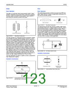
Figure AN1001.1 shows the simple block construction of an SCR.
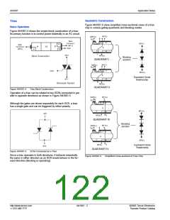
Geometric Construction
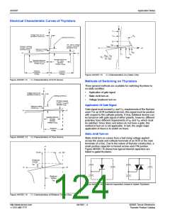
Figure AN1001.3 shows cross-sectional views of an SCR chip
and illustrations of current flow and junction biasing in both the
blocking and triggering modes.
Anode
Anode
P
J1
Cathode
(-)
Gate
(+)
Cathode
(-)
N
P
N
I
J2
J3
GT
Forward
Blocking
Junction
Gate
Gate
N
P
Cathode
N
Cathode
P
Block Construction
Figure AN1001.1
Schematic Symbol
(+)
Anode
(+)
Anode
I
T
SCR Block Construction
The operation of a PNPN device can best be visualized as a spe-
cially coupled pair of transistors as shown in Figure AN1001.2.
Equivalent Diode
Relationship
Forward Bias and Current Flow
Load
Anode
Anode
P
Cathode
(+)
Gate
P
Cathode
(+)
Reverse Biased
Gate Junction
P
N
P
N
J1
J2
N
N
P
N
J2
J3
Gate
N
P
N
N
P
Gate
Reverse Biased
Junction
(-)
(-)
Cathode
Anode
Anode
Cathode
Equivalent Diode
Relationship
Reverse Bias
Two-transistor
Schematic
Two-transistor Block
Construction Equivalent
Figure AN1001.2
Coupled Pair of Transistors as a SCR
Figure AN1001.3
Cross-sectional View of SCR Chip
©2002 Teccor Electronics
Thyristor Product Catalog
AN1001 - 1
http://www.teccor.com
+1 972-580-7777

 TECCOR [ TECCOR ELECTRONICS ]