Document Number: PS-MPU-6500A-01
Revision: 1.1
Release Date: 03/05/2014
MPU-6500 Product Specification
1.2 Purpose and Scope
This document is a preliminary product specification, providing a description, specifications, and design
related information on the MPU-6500™ MotionTracking device. The device is housed in a small 3x3x0.90mm
QFN package.
Specifications are subject to change without notice. Final specifications will be updated based upon
characterization of production silicon. For references to register map and descriptions of individual registers,
please refer to the MPU-6500 Register Map and Register Descriptions document.
1.3 Product Overview
The MPU-6500 is a 6-axis MotionTracking device that combines a 3-axis gyroscope, 3-axis accelerometer,
and a Digital Motion Processor™ (DMP) all in a small 3x3x0.9mm package. It also features a 512-byte FIFO
that can lower the traffic on the serial bus interface, and reduce power consumption by allowing the system
processor to burst read sensor data and then go into a low-power mode. With its dedicated I2C sensor bus,
the MPU-6500 directly accepts inputs from external I2C devices. MPU-6500, with its 6-axis integration, on-
chip DMP, and run-time calibration firmware, enables manufacturers to eliminate the costly and complex
selection, qualification, and system level integration of discrete devices, guaranteeing optimal motion
performance for consumers. MPU-6500 is also designed to interface with multiple non-inertial digital
sensors, such as pressure sensors, on its auxiliary I2C port.
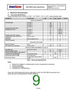
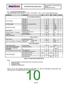
The gyroscope has a programmable full-scale range of ±250, ±500, ±1000, and ±2000 degrees/sec and very
low rate noise at 0.01 dps/√Hz. The accelerometer has a user-programmable accelerometer full-scale range
of ±2g, ±4g, ±8g, and ±16g. Factory-calibrated initial sensitivity of both sensors reduces production-line
calibration requirements.
Other industry-leading features include on-chip 16-bit ADCs, programmable digital filters, a precision clock
with 1% drift from -40°C to 85°C, an embedded temperature sensor, and programmable interrupts. The
device features I2C and SPI serial interfaces, a VDD operating range of 1.71 to 3.6V, and a separate digital
IO supply, VDDIO from 1.71V to 3.6V.
Communication with all registers of the device is performed using either I2C at 400kHz or SPI at 1MHz. For
applications requiring faster communications, the sensor and interrupt registers may be read using SPI at
20MHz.
By leveraging its patented and volume-proven CMOS-MEMS fabrication platform, which integrates MEMS
wafers with companion CMOS electronics through wafer-level bonding, InvenSense has driven the package
size down to a footprint and thickness of 3x3x0.90mm (24-pin QFN), to provide a very small yet high
performance low cost package. The device provides high robustness by supporting 10,000g shock reliability.
1.4 Applications
•
•
•
•
•
•
•
•
TouchAnywhere™ technology (for “no touch” UI Application Control/Navigation)
MotionCommand™ technology (for Gesture Short-cuts)
Motion-enabled game and application framework
Location based services, points of interest, and dead reckoning
Handset and portable gaming
Motion-based game controllers
3D remote controls for Internet connected DTVs and set top boxes, 3D mice
Wearable sensors for health, fitness and sports
7 of 40

 TDK [ TDK ELECTRONICS ]