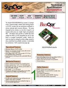
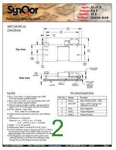
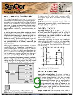
Input:
Output:
Current:
Package:
35-55 V
9.6 V
43 A
Quarter-brick
Technical Specification
BQ55090QPA40 ELECTRICAL CHARACTERISTICS
TA=25°C, airflow rate=300 LFM, Vin=48Vdc unless otherwise noted; full operating temperature range is -40°C to +100°C ambient tem-
perature with appropriate power derating. Specifications subject to change without notice.
Parameter
Min.
Typ.
Max.
Units Notes & Conditions
ABSOLUTE MAXIMUM RATINGS
Input Voltage
Non-Operating
60
55
V
V
Continuous
Operating
Continuous
Isolation Voltage (input to output)
Operating Temperature
2000
100
125
18
V
Basic insulation, Pollution Degree 2
-40
-55
-2
°C
°C
V
Storage Temperature
Voltage at ON/OFF input pin
INPUT CHARACTERISTICS
Operating Input Voltage Range
Input Under-Voltage Lockout
Turn-On Voltage Threshold
Turn-Off Voltage Threshold
Lockout Voltage Hysteresis
Input Over-Voltage Shutdown
Turn-Off Voltage Threshold
Turn-On Voltage Threshold
Maximum Input Current
35
48
55
V
30
29
2
34
31
4
V
V
V
58.5
57
59.5
58
V
V
9.5
0.13
15
A
100% Load, 35 Vin
No-Load Input Current
A
Disabled Input Current
7.0
mA
2
Inrush Current Transient Rating
Input Reflected Ripple Current
Input Terminal Ripple Current
Recommended Input Fuse
Input Filter Component Values (L\C)
Recommended External Input Capacitance
OUTPUT CHARACTERISTICS
Output Voltage Set Point
0.01
10
A s
7
mA
mA
A
RMS through 10µH inductor; Figure 14
RMS; Figure 13
140
20
Fast blow external fuse recommended
0.22\11
47
µH\µF Internal values
µF
V
Typical ESR 0.1-0.2
Ω,
9.6
48Vin, no load
Output Voltage Regulation
Over Line
42\4.0
5.2\500
2\200
%\V
%\mV
%\mV
V
Over Load
Over Temperature
Total Output Voltage Range
Output Voltage Ripple and Noise
Peak-to-Peak
6.5
0
11.0
100
43
Over sample, line, load, temperature & life
20MHz bandwidth
50
12
mV
mV
A
Full Load; see Figure 15
Full Load
RMS
Operating Output Current Range
Output DC Current-Limit Inception
Output DC Current-Limit Shutdown Voltage
Current Share Accuracy (3 units paralleled)
Back-Drive Current Limit while Disabled
Maximum Output Capacitance
DYNAMIC CHARACTERISTICS
Input Voltage Ripple Rejection
Output Voltage during Load Current Transient
For a Step Change in Output Current (0.1A/µs)
Settling Time
Subject to derating
50
5
A
V
+
10
%
Above 50% of rated output current
Negative current drawn from output
9.6Vout at 40A Resistive Load
10
mA
µF
4,000
14
dB
Figure 19
200
100
mV
µs
50%-75%-50% Iout max; Figure 11
To within 1% Vout nom
Turn-On Transient
Turn-On Time (without output capacitance)
Turn-On Time (with output capacitance)
Output Voltage Overshoot
EFFICIENCY
250
5
µs
ms
%
Full load, Vout=90% nom., 0 output cap.
Full load, Vout=90% nom., 3,000 µF cap.
3,000 µF load cap., Iout = 0A, Vin nom.
3
0
93% Load
96.5
97.0
%
%
Figure 1; 48Vin, 40A
Figure 1
50% Load
TEMPERATURE LIMITS FOR POWER DERATING CURVES
Semiconductor Junction Temperature (see Note 1)
Board Temperature
125
125
125
°C
°C
°C
Package rated to 175°C
Board rated to 165°C
Transformer Temperature
ISOLATION CHARACTERISTICS
Isolation Voltage (dielectric strength)
Isolation Resistance
2000
30
V
MΩ
1. For normal operating conditions of 55°C ambient temperature and 200 LFM airflow. Device is designed to operate for a minimum of 72 hours, once per
year under the following conditions: 70°C, 200 LFM airflow, 38Vin, 300W output power. Junction temperature during those conditions will exceed the listed
specification.
Product # BQ55090QPA40
Phone 1-888-567-9596
www.synqor.com
Doc.# 005-2BQ559K Rev. A
3/6/07
Page 3

 SYNQOR [ SYNQOR WORLDWIDE HEADQUARTERS ]