USBLC6-2
4. CROSSTALK BEHAVIOR
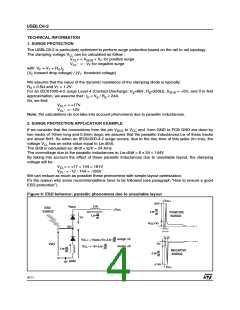
4.1. Crosstalk phenomena
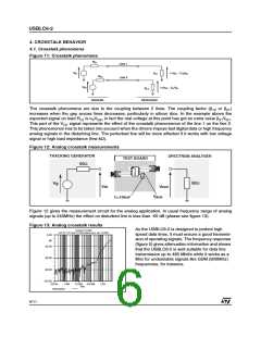
Figure 11: Crosstalk phenomena
RG1
Line 1
Line 2
VG1
α
1VG1
β
+
12VG2
RL1
RG2
VG2
α2
VG2
β
+
21VG1
RL2
DRIVERS
RECEIVERS
The crosstalk phenomena are due to the coupling between 2 lines. The coupling factor (β12 or β21)
increases when the gap across lines decreases, particularly in silicon dice. In the example above the
expected signal on load RL2 is α2VG2, in fact the real voltage at this point has got an extra value β21VG1
.
This part of the VG1 signal represents the effect of the crosstalk phenomenon of the line 1 on the line 2.
This phenomenon has to be taken into account when the drivers impose fast digital data or high frequency
analog signals in the disturbing line. The perturbed line will be more affected if it works with low voltage
signal or high load impedance (few kΩ).
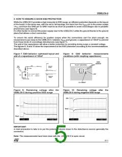
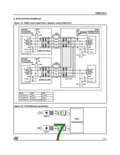
Figure 12: Analog crosstalk measurements
TRACKING GENERATOR
SPECTRUM ANALYSER
TEST BOARD
50Ω
50Ω
Vg
Vin
Vout
V
BUS
C=100nF
Figure 12 gives the measurement circuit for the analog application. In usual frequency range of analog
signals (up to 240MHz) the effect on disturbed line is less than -55 dB (please see figure 13).
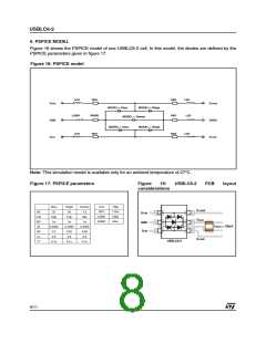
Figure 13: Analog crosstalk results
As the USBLC6-2 is designed to protect high
Analog Crosstalk
APLAC 7.91 User: ST Microelectronics Jan 12 2005
speed data lines, it must ensure a good transmis-
0.00
sion of operating signals. The frequency response
dB
(figure 5) gives attenuation information and shows
-30.00
that the USBLC6-2 is well suitable for data line
transmission up to 480 Mbit/s while it works as a
filter for undesirable signals like GSM (900MHz)
-60.00
frequencies, for instance.
-90.00
-120.00
100.0k
1.0M
10.0M
f/Hz
100.0M
1.0G
Attenuation
6/11

 STMICROELECTRONICS [ ST ]