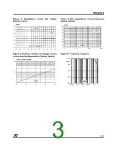
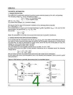
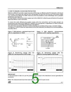
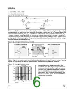
USBLC6-2
6. PSPICE MODEL
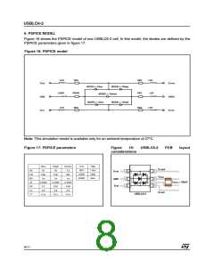
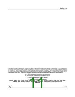
Figure 16 shows the PSPICE model of one USBLC6-2 cell. In this model, the diodes are defined by the
PSPICE parameters given in figure 17.
Figure 16: PSPICE model
LI/O
RI/O
RI/O
RI/O
LI/O
LI/O
D+in
GND
D-in
D+out
VBUS
D-out
MODEL = Dlow
MODEL = Dhigh
MODEL = Dhigh
LGND
RGND
MODEL = Dzener
MODEL = Dlow
LI/O
RI/O
RI/O
LI/O
Note: This simulation model is available only for an ambient temperature of 27°C.
Figure 17: PSPICE parameters Figure 18: USBLC6-2
PCB
layout
considerations
LI/O
RI/O
750p
110m
550p
60m
Dlow
50
Dhigh
50
Dzener
7.3
D+out
BV
CJ0
IBV
M
1
D+in
LGND
RGND
0.9p
1m
2.0p
1m
40p
V
BUS
1m
GND
D-in
CBUS = 100nF
0.3333
0.2
0.3333
0.52
0.6
0.3333
0.84
0.6
RS
VJ
0.6
D-out
USBLC6-2
TT
0.1u
0.1u
0.1u
8/11

 STMICROELECTRONICS [ ST ]