USBLC6-2
TECHNICAL INFORMATION
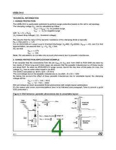
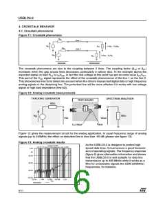
1. SURGE PROTECTION
The USBLC6-2 is particularly optimized to perform surge protection based on the rail to rail topology.
The clamping voltage VCL can be calculated as follow :
VCL+ = VBUS + VF for positive surge
V
CL- = - VF for negative surge
with: VF = VT + Rd.Ip
(VF forward drop voltage) / (VT threshold voltage)
We assume that the value of the dynamic resistance of the clamping diode is typically:
Rd = 0.5Ω and VT = 1.2V.
For an IEC61000-4-2 surge Level 4 (Contact Discharge: Vg=8kV, Rg=330Ω), VBUS = +5V, and if in first
approximation, we assume that : Ip = Vg / Rg = 24A.
So, we find:
V
V
CL+ = +17V
CL- = -12V
Note: the calculations do not take into account phenomena due to parasitic inductances.
2. SURGE PROTECTION APPLICATION EXAMPLE
If we consider that the connections from the pin VBUS to VCC and from GND to PCB GND are done by
two tracks of 10mm long and 0.5mm large; we assume that the parasitic inductances Lw of these tracks
are about 6nH. So when an IEC61000-4-2 surge occurs, due to the rise time of this spike (tr=1ns), the
voltage VCL has an extra value equal to Lw.dI/dt.
The dI/dt is calculated as: dI/dt = Ip/tr = 24 A/ns
The overvoltage due to the parasitic inductances is: Lw.dI/dt = 6 x 24 = 144V
By taking into account the effect of these parasitic inductances due to unsuitable layout, the clamping
voltage will be :
V
V
CL+ = +17 + 144 = 161V
CL- = -12 - 144 = -156V
We can reduce as much as possible these phenomena with simple layout optimization.
It’s the reason why some recommendations have to be followed (see paragraph “How to ensure a good
ESD protection”).
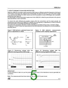
Figure 6: ESD behavior; parasitic phenomena due to unsuitable layout
V
CL
+
183V
di
Lw
di
V
BUS
ESD
SURGE
+V
CC
Lw
POSITIVE
SURGE
dt
Lw
V
F
dt
V +V
CC F
t
I/O
tr=1ns
tr=1ns
di
dt
surge >0
surge <0
V + = V +V +Lw
CL BUS F
t
-V
F
VI/O
di
dt
V
- = -V -Lw
CL F
di
dt
Lw
NEGATIVE
SURGE
di
dt
-Lw
GND
-178V
V
CL
-
4/11

 STMICROELECTRONICS [ ST ]