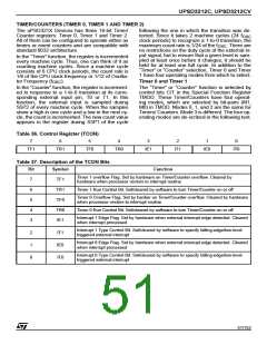
UPSD3212C, UPSD3212CV
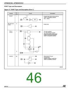
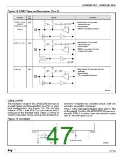
Figure 18. PORT Type and Description (Part 2)
In/
Out
Symbol
Circuit
Function
PORT1 <3:0>,
PORT3,
PORT4<7:3,1:0>
Bidirectional I/O port with
internal pull-ups
Schmitt input
I/O
CMOS compatible interface
PORT2
Bidirectional I/O port with
internal pull-ups
PORT1 < 7:4 >
I/O
Schmitt input
CMOS compatible interface
Analog input option
an_enb
Bidirectional I/O port with internal
pull-ups
I/O
PORT4.2
Schmitt input.
TTL compatible interface
AI07428
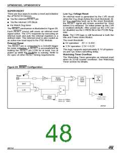
OSCILLATOR
The oscillator circuit of the uPSD321X Devices is
a single stage inverting amplifier in a Pierce oscil-
lator configuration (see Figure 19). The circuitry
between XTAL1 and XTAL2 is basically an invert-
er biased to the transfer point. Either a crystal or
ceramic resonator can be used as the feedback el-
ement to complete the oscillator circuit. Both are
operated in parallel resonance.
XTAL1 is the high gain amplifier input, and XTAL2
is the output. To drive the uPSD321X Devices ex-
ternally, XTAL1 is driven from an external source
and XTAL2 left open-circuit.
Figure 19. Oscillator
XTAL1
XTAL2
XTAL1
XTAL2
8 to 40 MHz
External Clock
AI06620
47/152

 STMICROELECTRONICS [ ST ]