UPSD3212C, UPSD3212CV
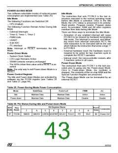
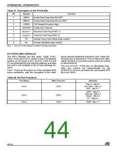
Table 27. Description of the PCON Bits
Bit
7
Symbol
SMOD
Function
Double Baud Data Rate Bit UART
Double Baud Data Rate Bit 2nd UART
LVR Disable Bit (active High)
Enable ADC Interrupt
6
SMOD1
LVREN
5
4
ADSFINT
(1)
3
Received Clock Flag (UART 2)
RCLK1
(1)
2
1
0
Transmit Clock Flag (UART 2)
TCLK1
PD
Activate Power-down Mode (High enable)
Activate Idle Mode (High enable)
IDL
Note: 1. See the T2CON register for details of the flag description
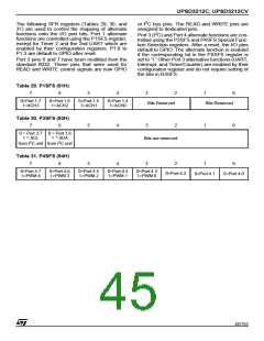
I/O PORTS (MCU MODULE)
The MCU Module has five ports: Port0, Port1,
Port2, Port3 and Port 4. (Refer to the PSD Module
section on I/O ports A,B,C and D). Ports P0 and
P2 are dedicated for the external address and data
bus and is not available in the 52-pin package de-
vices.
tional special peripheral functions (see Table 28).
All ports are bi-directional. Pins of which the alter-
native function is not used may be used as normal
bi-directional I/O.
The use of Port1- Port4 pins as alternative func-
tions are carried out automatically by the
uPSD321X Devices provided the associated SFR
Bit is set HIGH.
Port1 - Port3 are the same as in the standard 8032
micro-controllers, with the exception of the addi-
Table 28. I/O Port Functions
Port Name
Main Function
Alternate
Timer 2 - Bits 0,1
2nd UART - Bits 2,3
ADC - Bits 4..7
Port 1
GPIO
UART - Bits 0,1
Interrupt - Bits 2,3
Timers - Bits 4,5
Port 3
Port 4
GPIO
GPIO
2
I C - Bits 6,7
PWM - Bits 3..7
44/152

 STMICROELECTRONICS [ ST ]