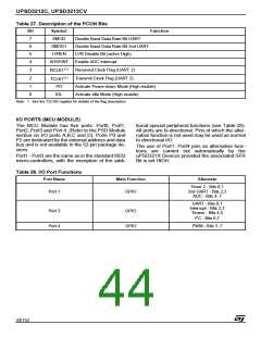
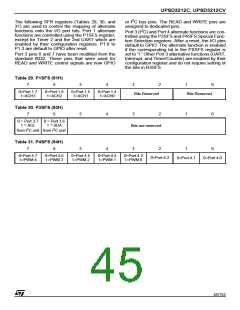
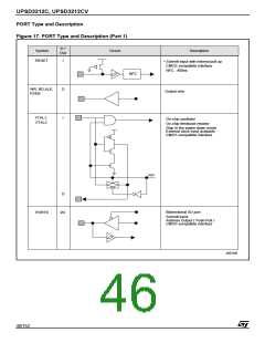
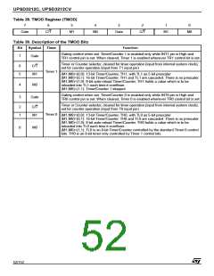
UPSD3212C, UPSD3212CV
SUPERVISORY
There are four ways to invoke a reset and initialize
the uPSD321X Devices.
Low V Voltage Reset
An internal reset is generated by the LVR circuit
DD
■ Via the external RESET pin
■ Via the internal LVR Block.
when the V drops below the reset threshold. Af-
DD
ter V
reaching back up to the reset threshold,
DD
the RESET signal will remain asserted for 10ms
before it is released. On initial power-up the LVR
is enabled (default). After power-up the LVR can
be disabled via the LVREN Bit in the PCON Reg-
ister.
Note: The LVR logic is still functional in both the
Idle and Power-down Modes.
■ Via Watch Dog timer
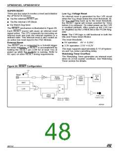
The RESET mechanism is illustrated in Figure 20.
Each RESET source will cause an internal reset
signal active. The CPU responds by executing an
internal reset and puts the internal registers in a
defined state. This internal reset is also routed as
an active low reset input to the PSD Module.
The reset threshold:
■ 5V operation: 4V +/- 0.25V
External Reset
The RESET pin is connected to a Schmitt trigger
for noise reduction. A RESET is accomplished by
holding the RESET pin LOW for at least 1ms at
power up while the oscillator is running. Refer to
AC spec on other RESET timing requirements.
■ 3.3V operation: 2.5V +/-0.2V
This logic supports approximately 0.1V of hystere-
sis and 1µs noise-cancelling delay.
Watchdog Timer Overflow
The Watchdog Timer generates an internal reset
when its 22-bit counter overflows. See Watchdog
Timer section for details.
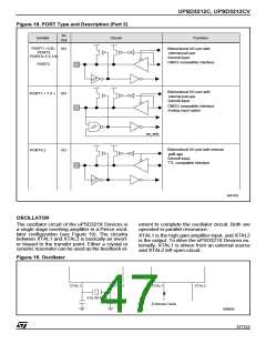
Figure 20. RESET Configuration
Reset
CPU
&
Noise
Cancel
CPU
Clock
PERI.
Sync
WDT
LVR
S
Q
R
10ms
Timer
PSD_RST
“Active Low
10ms at 40Mhz
50ms at 8Mhz
AI07429
48/152

 STMICROELECTRONICS [ ST ]