Electrical specifications and characteristics
TDA7719
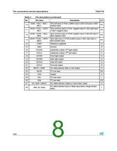
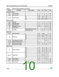
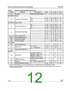
Table 5.
Symbol
VDC
Electrical characteristics (continued)
Parameter Test condition
Min.
Typ.
Max.
Unit
DC steps
Adjacent attenuation steps
0.1
5
mV
Subwoofer lowpass
fLP1
fLP2
fLP3
72
80
88
Hz
Hz
Hz
(2)
fLP
Lowpass corner frequency
108
144
120
160
132
176
DC offset detection circuit
V2
V3
V4
20
30
60
5
50
75
100
11
22
33
44
5
80
110
140
25
mV
mV
mV
µs
Vth
Zero comp window size
10
15
20
1
50
µs
tsp
Max rejected spike length
75
µs
100
10
µs
ICHDCErr
IDISDCErr
VOutH
DCErr charge current
DCErr discharge current
DCErr high volotage
DCErr low voltage
µA
mA
V
3.5
3
5
6.5
3.6
300
3.3
100
VOutH
mV
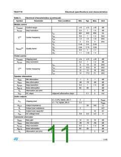
Level meter
Vout
Output voltage range
Output level
0
3.4
2.0
0.5
V
V
Vin = 1Vrms
1.2
-0.5
1.6
0
VLEVEL
Vin = AC Grounded
V
TDEL
Analog output delay time
2
µs
General
BW=20Hz to 20kHz A-
Weighted, all gain = 0dB
12
6
30
25
µV
µV
dB
eNO
S/N
Output noise
BW=20Hz - 20kHz A-
Weighted, Output muted
all gain = 0dB, A-weighted;
Vo = 2VRMS
Signal to noise ratio
104
D
Distortion
V
IN =1VRMS; all stages 0dB
0.01
90
0.2
%
SC
Channel separation left/right
80
dB
1. When DC offset detector is not used, the impedance of mono single-ended input is 50kΩ instead of 100kΩ
2. Minimun, typical and maximum are calculate in according to simulation result. Functionality is guaranteed by measuring a
directly correlated parameter.
12/45

 STMICROELECTRONICS [ ST ]