Description
TDA7719
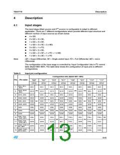
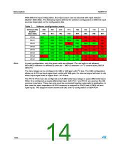
With different input configuration, the input source can be selected with input selector
(Byte0/1 Bit0~Bit2). The following matrix defines the selector configuration of different input
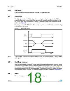
sources dependant on the configuration bits.
Table 7.
Selector configuration matrix
Selector Bits
(Byte0/1
Bit2~Bit0)
000
001
010
011
IN3
100
IN4
101
IN5
110
IN6
111
IN7
IN0
IN1
IN2
CFG0
CFG1
CFG2
CFG3
CFG4
CFG5
CFG6
CFG7
QD1
QD2
SE3
SE3
SE3
QD2
QD2
SE3
SE3
QD3
QD3
QD3
QD3
QD3
QD3
QD3
QD3
QD4
QD4
NA
NA
SE2
SE2
SE2
NA
NA
NA
NA
NA
NA
NA
NA
NA
NA
NA
MD3
NA
SE1
SE1
SE1
QD1
QD1
NA
SE4
NA
SE5
NA
MD1/2
FD
NA
NA
NA
NA
SE4
NA
SE5
NA
FD
SE2
SE2
SE1
FD
NA
NA
Note:
In each configuration, only the green cells are allowed. The red cells is not allowed.
MD1/MD2 selection is defined by extra bit – ‘MD1/2 selection’ in I C control table (Bit3 of
Byte0/1).
2
2
The input stage can be configured to 0dB or 3dB gain with I C bus. The 0dB configuration
allows up to 2Vrms input signal level, while with 3dB gain, the internal signal will start to clip
when input signal level is higher than 1.414Vrms.
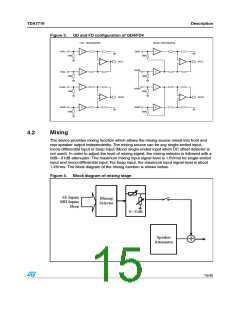
The Pin10~Pin13 can be configured as full differential input stage or quasi-differential input.
When it is configured as quasi-differential input, both Pin11 and Pin12 are used as the QD
common input pins. These two pins must be connected together externally in application. In
this case the input impedance of QD4 common is reduced to 50kΩ (half of QD4 left and
right input). The diagram below shows both QD and FD configuration of QD4/FD4.
14/45

 STMICROELECTRONICS [ ST ]