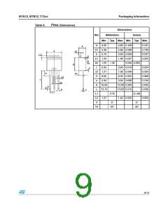
BTA12, BTB12, T12xx
Characteristics
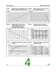
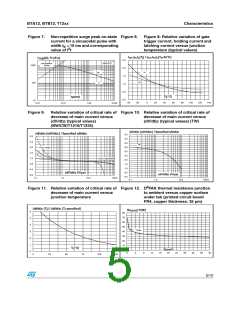
Figure 7.
Non-repetitive surge peak on-state Figure 8.
current for a sinusoidal pulse with
Figure 8: Relative variation of gate
trigger current, holding current and
latching current versus junction
temperature (typical values)
width t < 10 ms and corresponding
p
2
value of I t
(A), I2t (A2s)
I
,I ,I [T ] / I ,I ,I [T =25°C]
GT
H
L
j
GT
H
L
j
I
TSM
2.5
2.0
1.5
1.0
0.5
0.0
Tj initial=25°C
dI/dt limitation:
50A/µs
1000
100
10
ITSM
IGT
IH & IL
I2t
T (°C)
j
t (ms)
p
-40
-20
0
20
40
60
80
100
120
140
0.01
0.10
1.00
10.00
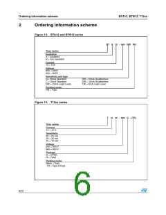
Figure 9.
Relative variation of critical rate of Figure 10. Relative variation of critical rate of
decrease of main current versus
(dV/dt)c (typical values)
decrease of main current versus
(dV/dt)c (typical values) (TW)
(BW/CW/T1210/T1235)
(dI/dt)c [(dV/dt)c] / Specified (dI/dt)c
(dI/dt)c [(dV/dt)c] / Specified (dI/dt)c
5.0
4.5
4.0
3.5
3.0
2.5
2.0
1.5
1.0
0.5
0.0
2.8
2.4
2.0
1.6
1.2
0.8
0.4
0.0
TW
T1210/SW
C
B
T1235/T1250/CW/BW
(dV/dt)c (V/µs)
(dV/dt)c (V/µs)
0.1
1.0
10.0
100.0
0.1
1.0
10.0
100.0
2
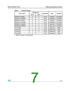
Figure 11. Relative variation of critical rate of Figure 12. D PAK thermal resistance junction
decrease of main current versus
junction temperature
to ambient versus copper surface
under tab (printed circuit board
FR4, copper thickness: 35 µm)
(dI/dt)c [T ] / (dI/dt)c [T specified]
j
j
R
(°C/W)
th(j-a)
6
5
4
3
2
1
0
80
70
60
50
40
30
20
10
0
D2PAK
T (°C)
j
S(cm²)
20
0
4
8
12
16
24
28
32
36
40
0
25
50
75
100
125
5/12

 STMICROELECTRONICS [ ST ]