Characteristics
BTA12, BTB12, T12xx
1
Characteristics
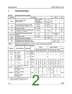
Table 2.
Absolute maximum ratings
Symbol
Parameter
I2PAK / D2PAK /
Value
Unit
Tc = 105° C
RMS on-state current
(full sine wave)
TO-220AB
TO-220AB Ins.
F = 50 Hz
IT(RMS)
12
A
Tc = 90° C
t = 20 ms
120
126
78
Non repetitive surge peak on-state
current (full cycle, Tj initial = 25° C)
ITSM
A
F = 60 Hz
t = 16.7 ms
I2t
I2t Value for fusing
tp = 10 ms
A s
²
Critical rate of rise of on-state current
IG = 2 x IGT , tr ≤ 100 ns
dI/dt
F = 120 Hz
Tj = 125° C
Tj = 25° C
50
A/µs
V
Non repetitive surge peak off-state
voltage
VDRM/VRRM
+ 100
V
DSM/VRSM
tp = 10 ms
tp = 20 µs
IGM
Peak gate current
Tj = 125° C
Tj = 125° C
4
1
A
PG(AV)
Average gate power dissipation
W
Tstg
Tj
Storage junction temperature range
Operating junction temperature range
- 40 to + 150
- 40 to + 125
°C
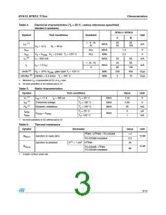
Table 3.
Electrical characteristics (T = 25°C, unless otherwise specified)
j
Snubberless and logic level (3 quadrants)
T12xx
BTA12 / BTB12
Symbol
Test conditions
Quadrant
Unit
T1210 T1235 T1250 TW
SW CW BW
(1)
IGT
I - II - III MAX.
I - II - III MAX.
10
35
50
5
10
35
50
mA
V
VD = 12 V
RL = 30 Ω
VGT
VGD
1.3
0.2
VD = VDRM
RL = 3.3 kΩ
Tj = 125° C
I - II - III
MIN.
V
(2)
IH
IT = 100 mA
MAX.
MAX.
15
25
30
35
50
60
50
70
80
10
10
15
15
25
30
35
50
60
50
70
80
mA
mA
I - III
II
IL
IG = 1.2 IGT
VD = 67 %VDRM gate open
Tj = 125° C
dV/dt (2)
MIN.
40
6.5
2.9
500
1000
20
3.5
1
40
6.5
2.9
500 1000 V/µs
(dV/dt)c = 0.1 V/µs
Tj = 125° C
(dV/dt)c = 10 V/µs
Tj = 125° C
(dI/dt)c (2)
MIN.
A/ms
Without snubber
Tj= 125° C
6.5
12
6.5
12
1. Minimum IGT is guaranted at 5% of IGT max
2. for both polarities of A2 referenced to A1
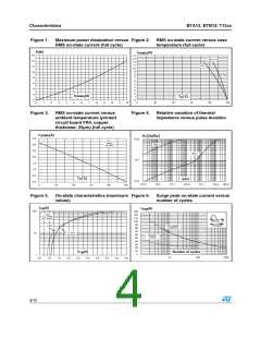
2/12

 STMICROELECTRONICS [ ST ]