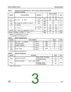
Characteristics
BTA12, BTB12, T12xx
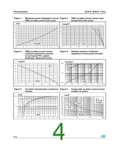
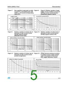
Figure 1.
Maximum power dissipation versus Figure 2.
RMS on-state current (full cycle)
RMS on-state current versus case
temperature (full cycle)
P(W)
I (A)
T(RMS)
16
14
13
12
11
10
9
BTB / T12
14
12
10
8
BTA
8
7
6
6
5
4
4
3
2
2
I (A)
T(RMS)
1
T (°C)
C
0
0
0
25
50
75
100
125
0
1
2
3
4
5
6
7
8
9
10
11
12
Figure 3.
RMS on-state current versus
ambient temperature (printed
circuit board FR4, copper
thickness: 35µm) (full cycle)
Figure 4.
Relative variation of thermal
impedance versus pulse duration
I
(A)
T(RMS)
K=[Z /R
]
th th
3.5
3.0
2.5
2.0
1.5
1.0
0.5
0.0
1E+0
1E-1
1E-2
D2PAK
Z
th(j-c)
(S=1cm2)
Z
th(j-a)
T (°C)
C
t (s)
p
1E-3
1E-2
1E-1
1E+0
1E+1
1E+2
5E+2
0
25
50
75
100
125
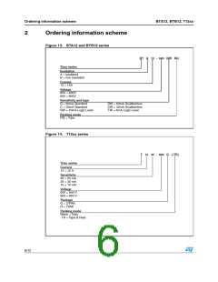
Figure 5.
On-state characteristics (maximum Figure 6.
values)
Surge peak on-state current versus
number of cycles
I
(A)
TM
I (A)
TSM
100
130
120
110
100
90
Tj max.
Vto = 0.85V
Rd = 35 mΩ
t=20ms
One cycle
Tj = Tj max.
Non repetitive
Tj initial=25°C
80
70
Tj = 25°C.
10
60
Repetitive
TC=90°C
50
40
30
20
10
V
(V)
TM
Number of cycles
0
1
1
10
100
1000
0.5
1.0
1.5
2.0
2.5
3.0
3.5
4.0
4.5
5.0
4/12

 STMICROELECTRONICS [ ST ]