PDF
最近搜索
热门搜索
发布采购

| 型号: | STM8S903K3T6C |
| PDF下载: | 下载PDF文件 查看货源 |
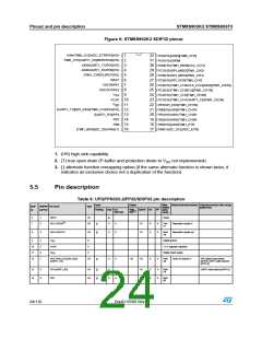
| 内容描述: | 16兆赫STM8S 8位MCU ,高达8 KB闪存, 1 KB的RAM , 640字节EEPROM , 10位ADC ,2个定时器, UART , SPI , I²C [16 MHz STM8S 8-bit MCU, up to 8 Kbytes Flash, 1 Kbyte RAM, 640 bytes EEPROM,10-bit ADC, 2 timers, UART, SPI, I²C] |
| 分类和应用: | 闪存微控制器和处理器外围集成电路可编程只读存储器电动程控只读存储器电可擦编程只读存储器时钟 |
| 文件页数/大小: | 116 页 / 1017 K |
| 品牌: |  STMICROELECTRONICS [ ST ] STMICROELECTRONICS [ ST ] |
专业IC领域供求交易平台:提供全面的IC Datasheet资料和资讯,Datasheet 1000万数据,IC品牌1000多家。